[News] World’s First Mass-Production Line for 6-/8-Inch Homoepitaxial Gallium Oxide Wafers Comes Online
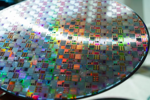
On June 24, 2026, Hangzhou Garen Semiconductor announced a major commercialization milestone: the company has successfully established the world’s first mass-production line compatible with both 6-inch and 8-inch homoepitaxial gallium oxide wafers. The company has already delivered 6-inch (100)-oriented homoepitaxial gallium oxide wafers to leading chipmakers, marking its entry into stable volume production and supply.
The global gallium oxide industry has long been constrained by small wafer sizes, limited production capacity, and poor uniformity. Most commercially available products have been restricted to 2-inch to 4-inch wafers, making large-scale manufacturing of advanced power devices difficult.
By establishing a complete mass-production process, Garen claims to have overcome key commercialization barriers and become the world’s first—and currently only—supplier capable of commercially delivering 6-inch homoepitaxial gallium oxide wafers.
The production line combines Garen’s proprietary cast-growth single-crystal technology with an optimized MOCVD epitaxy process. The in-house crystal growth method enables the production of ultra-thick gallium oxide crystals, while an ultra-thin substrate process increases substrate output by three to four times compared with conventional approaches.
The technology also significantly reduces iridium consumption, lowering substrate costs by more than 80% per wafer and helping cut material costs for downstream device manufacturers.
Product qualification data released by the company show that its 6-inch homoepitaxial gallium oxide wafers feature epitaxial layers exceeding 10μm in thickness, with thickness variation below 1%. The high level of uniformity is expected to support improved yields for high-performance devices designed for high-voltage, high-frequency, and high-temperature applications.
On the manufacturing side, Garen has established a fully integrated production chain covering single-crystal growth, substrate processing, and homoepitaxy. The 6-/8-inch compatible production line has reportedly achieved stable and controllable batch quality. In addition to long-term supply agreements with major domestic chipmakers, the company said that several overseas enterprises and research institutions have also placed orders, accelerating commercial adoption.
Gallium oxide, an ultra-wide-bandgap semiconductor material, offers high breakdown field strength, low conduction losses, and strong high-temperature performance. It is considered a promising material for applications including high-voltage power grids, electric vehicles, photovoltaic energy storage systems, and advanced RF communications.
The transition to larger wafer sizes is expected to significantly improve manufacturing efficiency, with an 8-inch wafer capable of producing roughly four times as many chips as a 4-inch wafer, enhancing the economics of large-scale production.
(Photo credit: FREEPIK)


