[News] Intel 18A-P Enters Risk Production, Targets 9% Performance Gain With Potentially Shortened Ramp
Amid ongoing speculation that Apple could emerge as an early customer for Intel’s 18A-P process for future M-series chips, Intel appears to be taking another step toward that possibility. At the VLSI Symposium in Honolulu on Tuesday, the company confirmed that 18A-P has entered risk production, according to Reuters and CNBC.
As highlighted by CNBC, Intel rolled out its baseline 18A process for PC chips in early 2026 but has yet to secure a major external customer. Against that backdrop, industry observers cited in the report view 18A-P as a more meaningful proving ground for the company’s ability to win over leading-edge chip designers.
According to Wccftech, after fabricating Panther Lake on its 18A, Intel has confirmed at COMPUTEX 2026 that its next-generation Diamond Rapids Xeon processors will be manufactured on the 18A-P node.
18A-P Timeline Could Be Shortened
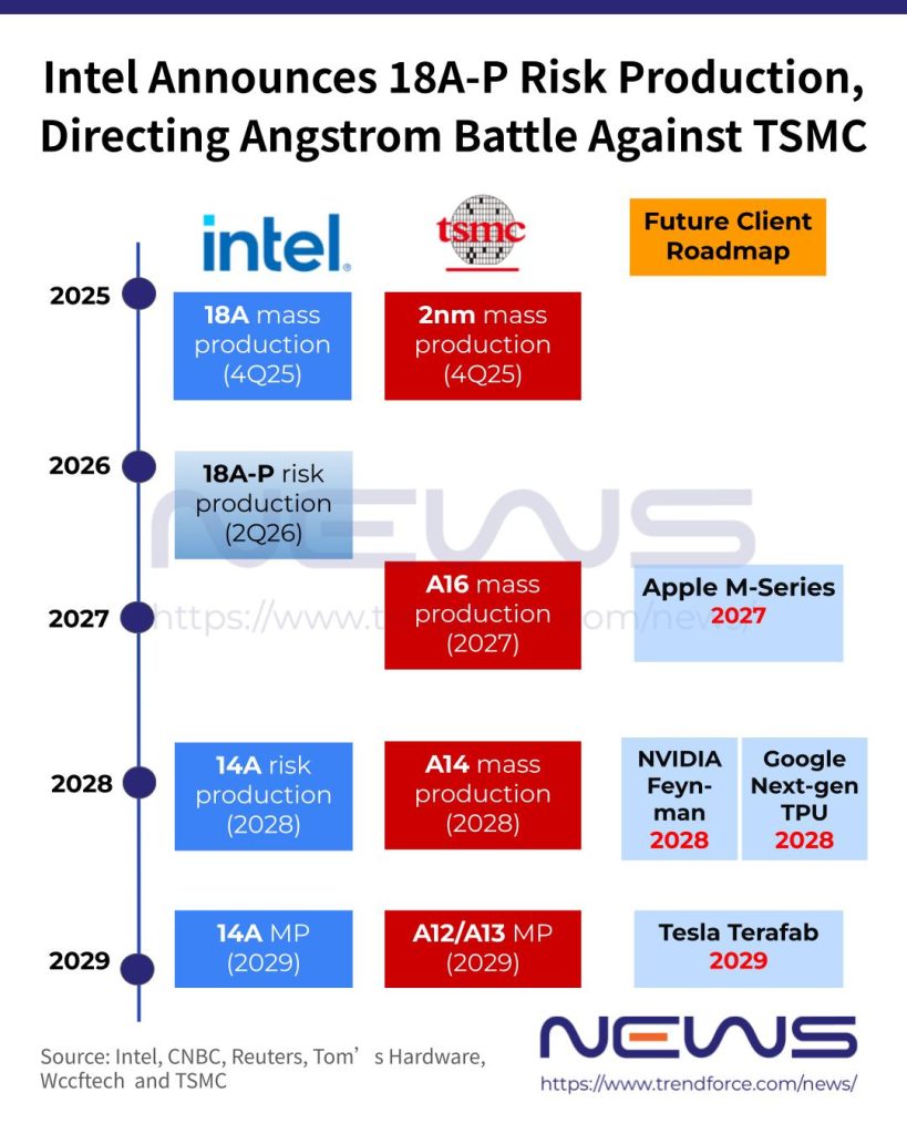
The move into risk production marks an early milestone on the path to volume manufacturing. According to Tom’s Hardware, while advanced logic nodes typically spend 12–24 months in risk production before reaching volume manufacturing, 18A-P could see a shorter ramp given its status as an evolution of the existing 18A process rather than a full node transition.
Beyond 18A-P, Intel’s roadmap continues to stretch further into the next generation. As noted by Wccftech earlier, CEO Lip-Bu Tan said Intel expects risk production for its 14A technology in 2028, followed by volume production in 2029, placing its timeline alongside TSMC’s.
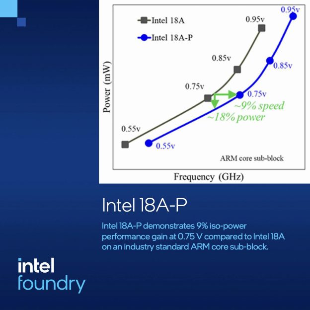
Intel Positions 18A-P as Upgrade Over 18A
Notably, Intel is positioning 18A-P as an incremental upgrade over its 18A process. According to CNBC, the company claims the node delivers up to 9% higher performance or 18% lower power consumption.
Wccftech reports that 18A-P is also being targeted at power-sensitive AI, HPC, and next-generation computing workloads. Beyond performance gains, Intel has introduced material-level enhancements, including a 20–40% improvement in thermal resistance when paired with advanced EDA optimizations, as well as a 10–30% reduction in through-silicon via (TSV) resistance, the report says.
In addition, Wccftech notes that the node retains Intel 18A’s gate-all-around (GAA) transistor and backside power architecture while maintaining full design-rule compatibility, enabling customers to reuse existing IP and design flows.
However, yields remain a challenge which should be closely watched. A previous CNBC report, citing CEO Lip-Bu Tan, said Intel’s foundry business is making progress, with 18A process yields improving by 7% to 8% per month. Separately, well-known analyst Jeff Pu said in early June that 18A yields have reached around 80%, while EMIB packaging yields are estimated at 90% to 95%.
Read more
- [News] Intel Foundry Gains Momentum as Google Reportedly Orders 3M TPUs, NVIDIA Evaluates 18A for Multi-Die GPUs
- [News] Intel Says 18A May Reach Strong Margins by 2027; Notebook Chips on the Node Mark Fastest Ramp in 5 Years
(Photo credit: Intel)