[News] Huawei, Xiaomi Reportedly Plan HBM-Inspired LLW DRAM for 2H27 to Boost On-Device AI in Smartphones
While smartphone form factors and thermal constraints have limited HBM adoption, Chinese smartphone brands are reportedly exploring HBM-inspired memory architectures. According to Wccftech, citing Weibo tipster Fixed-focus Digital, Xiaomi and Huawei may be planning to introduce custom Low Latency Wide DRAM (LLW) in 2H27. Although not true HBM, the design is said to address LPDDR performance bottlenecks, delivering higher performance with lower power consumption.
As the report highlights, LLW is rumored to offer 1.5x higher performance and 50% lower power consumption. While the benchmark was not specified, the report assumes the comparison is against LPDDR5X.
Mobile HBM Draws Interest Across the Smartphone Industry
The push for higher memory bandwidth in mobile AI workloads is also driving broader exploration of mobile HBM technologies. As CNMO highlights, Huawei could be among the first smartphone vendors to commercialize mobile HBM. The report notes that Huawei has significantly expanded its on-device AI efforts in recent years, while foldable devices—with their larger internal space—are better suited for testing technologies such as HBM. Industry sources have suggested that Huawei may be the first to introduce the technology in a foldable smartphone.
As for Apple, CNMO reports that sources expect the company to adopt mobile HBM around 2027, coinciding with the iPhone’s 20th anniversary. The report notes that on-device AI is a key pillar of Apple’s Apple Intelligence strategy. However, Apple’s ultra-thin design poses significant thermal challenges, making a highly customized implementation the more likely approach.
Meanwhile, Samsung appears to be making progress toward bringing HBM to mobile devices. ETNews, citing sources, reports that Samsung Electronics is developing next-generation HBM packaging technology for on-device AI, combining ultra-high-aspect-ratio copper pillars with FOWLP and advancing its VCS technology to enable high-capacity, high-bandwidth HBM in smartphones and tablets. While the commercialization timeline remains unclear, ETNews reports that the technology could appear in future Exynos chips, including later versions of the Exynos 2800 or Exynos 2900.
Challenges Remain for Mobile HBM Adoption
Despite its potential, HBM is unlikely to see widespread adoption in smartphones in the near term. As CNMO highlights, HBM currently costs roughly three to five times more to manufacture than LPDDR, while the smartphone industry remains highly sensitive to cost. Cameras, displays, satellite communications, AI chips, and thermal management systems are already placing pressure on device margins, and adding HBM would further increase bill-of-materials (BOM) costs.
Yield is another concern. The CNMO report notes that TSV and 3D stacking technologies involve significant manufacturing complexity, and advanced HBM solutions still face substantial yield challenges.
Read more
- [News] Huawei Unveils Pura 90 Pro Max with HyperSpace Memory, 12GB RAM Said to Match 16GB Performance
- [News] Samsung Reportedly Develops Mobile HBM Packaging With Copper Pillars, Bandwidth Up 15%–30%
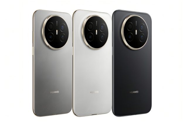
(Photo credit: Huawei)