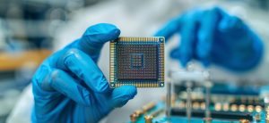
[News] MIT Announced Breakthrough in GaN-on-Single-Crystal Diamond Thermal Management Technology
On June 8, 2026, the Massachusetts Institute of Technology (MIT) announced that its researchers had successfully embedded gallium nitride (GaN) transistors into an ultra-thin single-crystal diamond layer, overcoming a major thermal bottleneck in high-power wireless chips and developing a record-setting wireless power amplifier.
The research was published at the IEEE International Microwave Symposium 2026, introducing a new chip-level thermal management approach for high-power electronic systems such as 6G communications and satellite internet infrastructure.
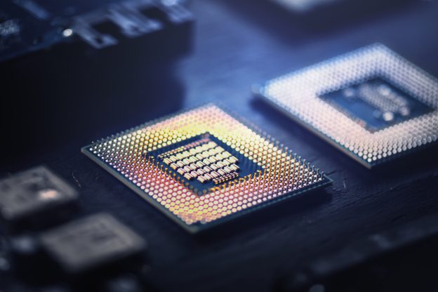
Conventional silicon-based chips face inherent limitations in power-handling capability, making it increasingly difficult to meet the performance and energy-efficiency requirements of next-generation high-speed wireless communications. As a wide-bandgap semiconductor, GaN offers superior power density and high-frequency operation, making it an ideal candidate for 6G networks, high-power radar systems, and satellite communications. However, GaN devices are prone to localized hotspots during operation, which can undermine reliability and restrict performance. Existing approaches that grow diamond layers on the device surface also face scalability challenges and introduce undesirable parasitic capacitance.
To address these issues, the MIT team developed a heterogeneous integration process that embeds micron-scale GaN transistor dielets into an ultra-thin single-crystal diamond interposer. Diamond, which possesses the highest thermal conductivity of any known material, rapidly dissipates heat, enabling the temperatures of GaN devices and adjacent silicon circuitry to remain closely aligned.
This significantly improves the reliability of three-dimensional integrated systems. Unlike conventional surface-coated diamond solutions, the new architecture eliminates parasitic capacitance, preserving high-frequency device performance.
Testing showed that wireless power amplifiers fabricated using the technology outperformed all comparable devices reported in the literature, establishing a new benchmark for performance. According to lead author Pradyot Yadav, a graduate researcher in MIT’s Department of Electrical Engineering and Computer Science, no single material can satisfy all performance requirements for future wireless systems.
As a result, three-dimensional heterogeneous integration is becoming an inevitable industry direction, while thermal management and reliability remain the key barriers to large-scale deployment. He noted that the breakthrough could help unlock broader adoption of high-power electronic systems.
The manufacturing process demands extremely high precision and involves the integration of multiple material systems, yet remains compatible with scalable commercial production. The technology is expected to support applications in the FR3 spectrum targeted for 6G communications, satellite internet equipment, high-power radar platforms, and data centers, while also providing a reusable thermal management architecture for next-generation high-power RF devices.
(Photo credit: FREEPIK)