[News] Applied Materials Opens $500M Singapore Site, Aims to Double Global Capacity on AI Demand
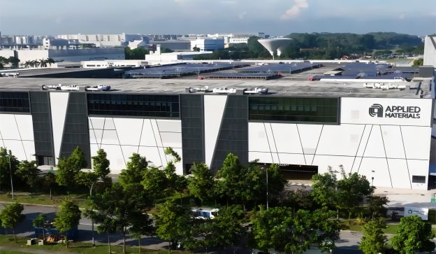
Applied Materials is expanding its footprint in Singapore as AI fuels semiconductor demand. According to Nikkei, the company has opened a US$500 million manufacturing campus there, a key part of its strategy to nearly double its global production capacity as AI accelerates semiconductor demand.
Gary Dickerson, president and CEO of Applied Materials, said the company’s semiconductor business is expected to grow by more than 30% this year and maintain a similar pace in the years ahead. He added that demand is expected to remain strong through 2027 and beyond.
The investment reflects accelerating demand for advanced chipmaking equipment. Dickerson said more than 80% of growth in wafer fab equipment is tied to leading-edge logic, memory, and advanced packaging.
As Nikkei notes, the new campus increases Applied Materials’ manufacturing sites in Singapore from one to three, making the city-state home to roughly half of the company’s global production capacity, with the remainder located in the U.S. According to CRN, the facility also includes a large-scale cleanroom, expanded production capacity, and R&D facilities serving global and regional customers. Applied Materials employs about 4,000 people in Singapore and plans to add another 1,000 local jobs in the coming years.
The company is also benefiting from greater visibility into future demand. Applied Materials’ major customers include TSMC, Intel, Samsung Electronics, SK hynix, and Micron. Dickerson said customers are increasingly sharing rolling eight-quarter forecasts, giving suppliers unprecedented visibility into demand and helping them better prepare for industry growth, Nikkei notes.
Applied Materials Bets on Long-Term AI-Driven Growth
Dickerson called AI the biggest inflection point of our lifetimes and said the industry is still in its early stages. According to Commercial Times, Applied Materials sees AI data centers driving the largest infrastructure investment cycle in history, with related spending expected to reach US$7 trillion over the next four to five years.
Prabu Raja, president of Applied Materials’ Semiconductor Products Group (SPG), said the AI era has shifted chip design priorities toward higher performance, lower power consumption, and faster time-to-market, with customers increasingly focused on energy-efficient computing, as cited by Commercial Times. He added that future process advances will hinge on major technology transitions such as GAA, backside power delivery, HBM, 3D DRAM, and advanced packaging.
Notably, advanced packaging is expected to be a key growth driver. According to Nikkei, Applied Materials expects revenue from advanced packaging equipment to increase 50% in 2026.
Read more
- [News] Applied Materials Eyes 25% Southeast Asia Hiring Growth, Mostly in Singapore, Advances Packaging Efforts
- [News] Applied Sees >30% Equipment Growth, >50% Packaging Surge in 2026; China Remains Top Market in 2Q
(Photo credit: Applied Materials)


