


[News] From 800 VDC to GPU Core: Innoscience All-GaN Technology Provides Key Solutions to High-Density AI Power Delivery for the NVIDIA MGX Ecosystem

AI reasoning, agentic workflows, and accelerated computing are transforming data centers into next-generation AI factories. As AI workloads scale from single servers to rack-scale systems and full data-center deployments, power delivery has become a critical enabler of system performance, efficiency, density, and total cost of ownership.
NVIDIA MGX™ is an open, modular reference architecture for AI factories, helping system builders develop future-compatible accelerated computing systems faster while reducing engineering cost and accelerating time to market. As a member of the NVIDIA MGX ecosystem, Innoscience recognizes MGX as an important industry platform for modular, scalable AI factory infrastructure and is advancing All-GaN power conversion technologies to support the next generation of high-density AI systems.
Power Delivery Becomes a Key AI Infrastructure Challenge
As rack power increases, the challenge is no longer only bringing power into the rack. The harder task is converting that power efficiently and compactly from high-voltage distribution down to the GPU core.
NVIDIA 800 VDC power architecture provides a practical path for higher-density AI infrastructure by reducing conversion stages and delivering DC power closer to the rack. However, converting from 800 VDC to low GPU operating voltages requires high efficiency, a high conversion ratio, compact magnetics, reduced thermal stress, and power devices capable of higher switching frequency.
Why GaN for AI Power?
GaN is becoming an important enabling technology for AI power delivery because it addresses several constraints that become more critical as rack power and GPU current continue to increase. Its low on-resistance, low gate charge, low parasitic capacitance, and zero reverse-recovery characteristics enable higher switching frequency, lower power loss, and more compact power-stage designs.
These device-level benefits translate into system-level value: smaller magnetics and passive components, improved thermal performance, higher power density, and lower overall system cost and TCO. Innoscience’s GaN-on-silicon technology combines these advantages with scalable manufacturing and a broad product portfolio. For AI infrastructure, Innoscience is building an All-GaN technology path that supports power conversion from 800 VDC distribution down to GPU core voltage.
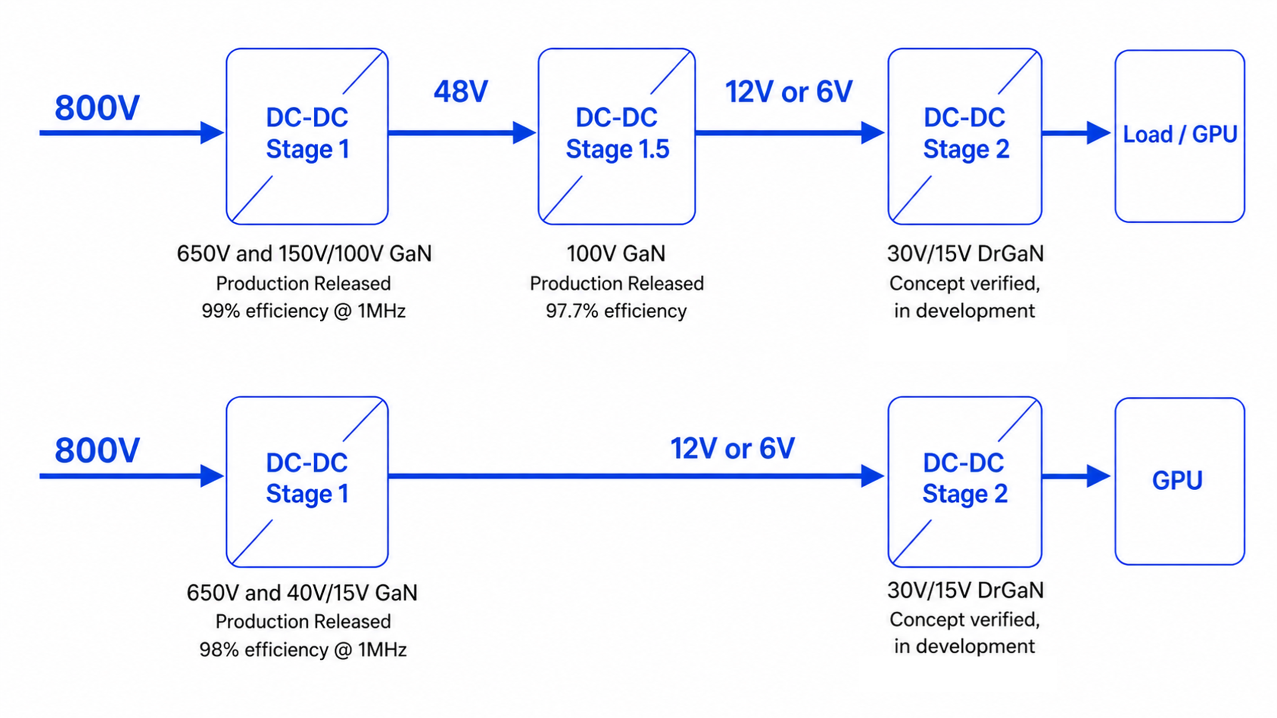 Figure 1. 800 VDC to GPU core voltage conversion stages and Innoscience All-GaN solution
Stage 1: High-Efficiency Front-End Conversion
As AI rack power continues scaling, the front-end conversion stage becomes one of the most demanding parts of the power architecture. It must simultaneously handle high input voltage, high conversion ratio, high power throughput, limited thermal budget, and increasingly constrained board space.
Innoscience’s latest All-GaN LLC solution demonstrates the benefits of GaN in this demanding front-end stage. In a 12 kW 800 V to 48 V-class design, Innoscience uses 650 V GaN 8×8 dual-side-cooling (DSC) devices on the primary side and 5×6 DSC 100 V GaN devices on the secondary side to enable high-frequency operation, low switching loss, and reduced conduction loss. The newly released 150 V GaN further simplifies the secondary side and reduces the required number of synchronous rectifier devices by 50%.
Innoscience’s latest data shows approximately 99% peak efficiency and 98.2% efficiency at full load. Innoscience’s All-GaN solution achieves this high efficiency at 1 MHz operation. The footprint reduction from high switching frequency operation is increasingly valuable as AI systems push toward higher rack density and more compact power shelves.
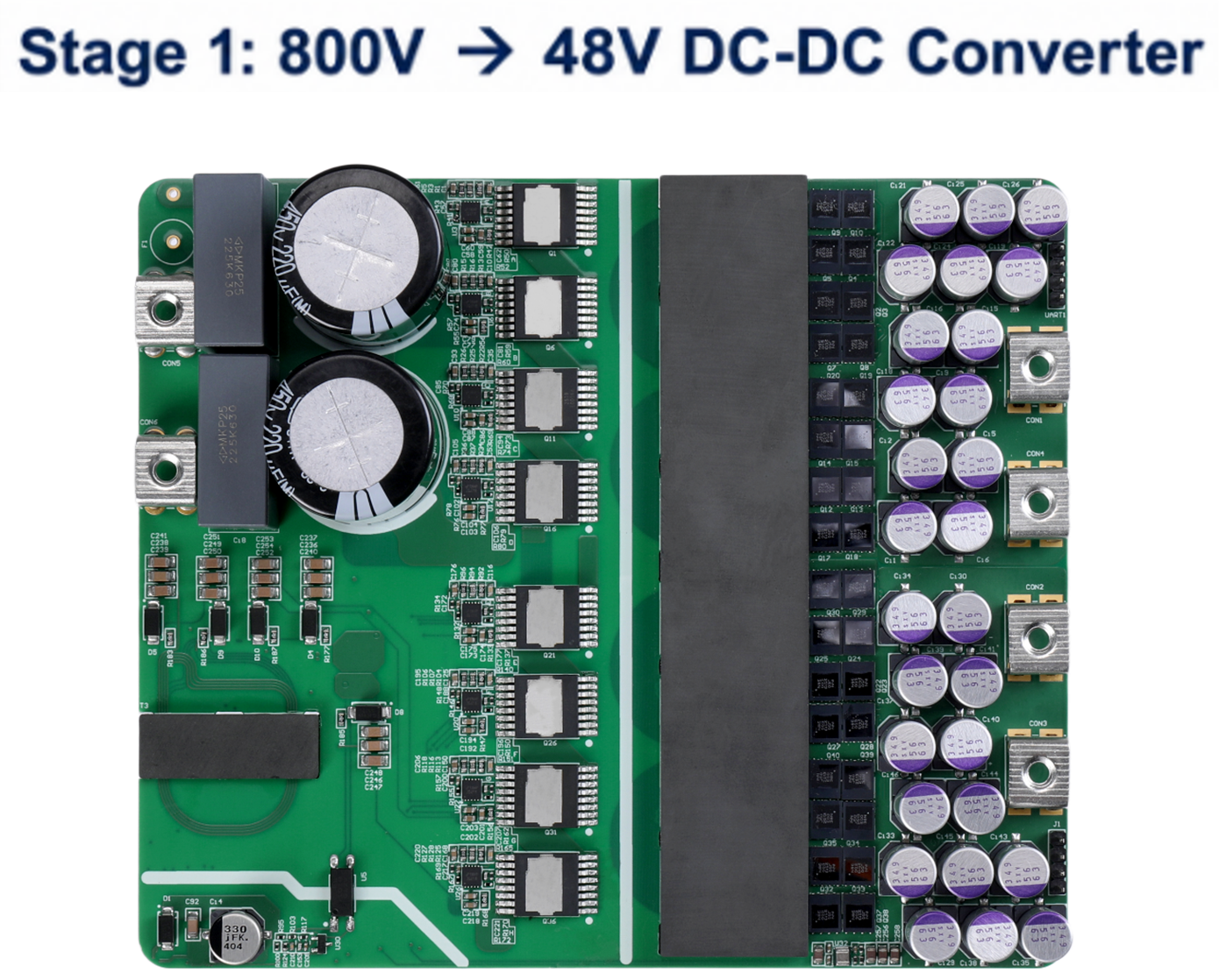 Figure 2. Innoscience 800 V to 48 V Demo
Expanding Coverage Across 800 VDC Architectures
Beyond the 800 V to 48 V front-end stage, Innoscience is expanding its All-GaN solution platform to cover the full range of intermediate bus voltage options required in next-generation AI power architectures, including 800 V to 48 V, 800 V to 12 V, and 800 V to 6 V conversion. This broader coverage gives system designers more flexibility to select the most suitable power architecture based on rack design, board space, thermal budget, and point-of-load requirements. For 800 V to 12 V conversion, Innoscience offers 40 V GaN devices in both 5×6 mm and compact 3.3×3.3 mm dual-side-cooling (DSC) packages, enabling high-efficiency synchronous rectification with reduced footprint and improved thermal performance. For 800 V to 6 V conversion, Innoscience provides 15 V GaN devices as the synchronous rectifier solution, supporting lower intermediate-bus architectures that can simplify the final conversion to GPU core voltage while maintaining the benefits of high-frequency, high-density GaN power delivery.
Stage 1.5: Scalable, High-Power-Density 48 V to 12 V Conversion
The 48 V to 12 V intermediate bus stage is another important building block in AI server power delivery. As accelerator platforms demand more power in less space, this stage must deliver high efficiency, high power density, and practical thermal performance.
Innoscience 100 V GaN solutions optimize 48 V to 12 V multiphase buck conversion. At AI-factory scale, even fractional efficiency improvements can translate into meaningful reductions in cooling requirements and operating cost. Intermediate bus architectures remain important building blocks in many MGX-compatible AI server designs, making this conversion stage a key target for GaN-enabled optimization.
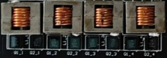
Figure 3. Power-density improvement enabled by Innoscience 100 V GaN
Stage 2: Dual-Channel DrGaN Enables Ultra-Low-Profile Vertical Power Delivery (VPD)
At the final conversion stage, where current demand is high and transient response is critical, vertical power delivery becomes an increasingly attractive architecture. As GPU current demand continues increasing, traditional lateral power delivery becomes increasingly challenging due to distribution loss, transient response limitations, and board routing complexity.
Vertical power delivery offers a promising path toward shorter current paths, lower parasitic loss, and higher current density. Innoscience has verified the feasibility of 15 V GaN HEMTs operating between 3 MHz and 5 MHz to reduce the size of the required magnetics and capacitors.
A DrGaN solution is currently in development at Innoscience. Support for high switching frequency significantly increases bandwidth for responding to fast GPU dynamic transients, while reducing the need for large amounts of traditional output capacitance.
As future MGX AI systems continue increasing accelerator current density, VPD-ready power stages can become an important building block for GPU near-core power delivery.
Innoscience GaN Portfolio and All-GaN Demo Platform
To support faster customer adoption, Innoscience provides a comprehensive portfolio of evaluation boards and reference designs that help system designers validate GaN performance across the AI power tree. Representative platforms include a 12 kW 800 V to 48 V PDB demo board, a 48 V to 12 V 4-phase GaN evaluation board, and an upcoming 6 V DrGaN evaluation board for future vertical power delivery architectures.
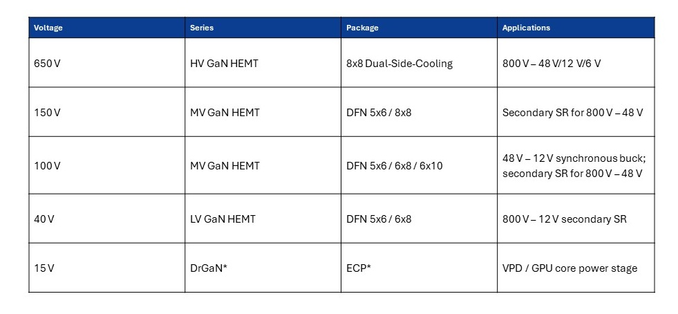 * Under Development
Enabling the Next Generation of AI Factories
The NVIDIA MGX ecosystem is helping accelerate the deployment of modular, scalable, and future-compatible AI infrastructure. As AI factories move toward higher rack power, greater compute density, and more efficient power architectures, power semiconductors must evolve as well.
Innoscience All-GaN technology is designed to support this transition. From 800 VDC to a 48 V-class intermediate bus, from 48 V to 12 V/6 V, and from 12 V/6 V to GPU core voltage, Innoscience GaN solutions enable higher switching frequency, lower loss, smaller passive components, and higher power density across the AI power delivery path. As AI infrastructure becomes increasingly power-constrained, Innoscience is committed to working with the NVIDIA MGX ecosystem to help advance higher-efficiency, higher-density, and more scalable AI power infrastructure.
(Photo credit: Innoscience)


