[News] TSMC Latest Roadmap: A12, A13 for 2029 Without High-NA EUV; A16 Volume Production Delayed to 2027
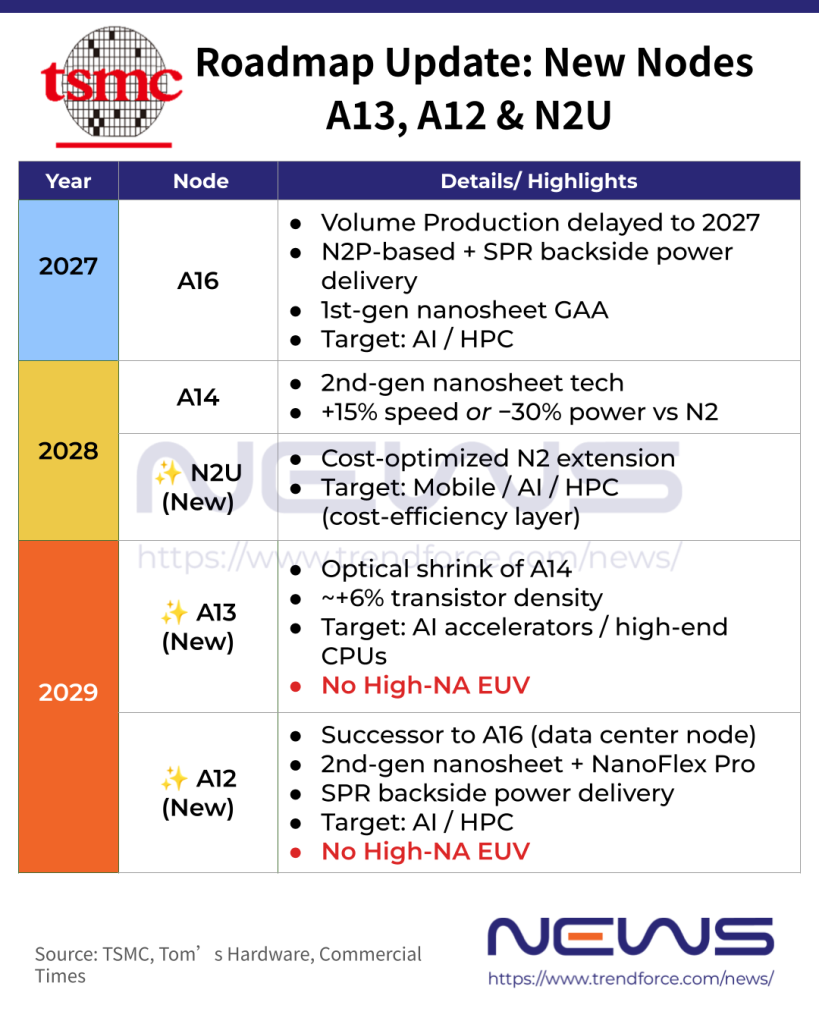
TSMC outlined its manufacturing technology roadmap through 2029 at its North American Technology Symposium 2026. According to Tom’s Hardware, the company introduced its 1.2nm- and 1.3nm-class processes, A12 and A13, both targeted for production in 2029, along with an unexpected extension of the N2 family, N2U. The report also notes that A16 volume production is now slated for 2027, marking a delay from its previously expected 2026 timeline.
For customers, A13 is expected to serve as a core option for next-generation AI accelerators and high-end CPUs, while A12 extends backside power delivery into more advanced computing products. N2U, meanwhile, fills the cost-efficiency gap across mobile, AI, and HPC segments, as noted by Commercial Times.
TSMC Expands Consumer Device Node Strategy with A13 and N2U
TSMC is set to introduce A13, an optical shrink of A14, targeted for production in 2029. As the Tom’s Hardware report indicates, A13 reduces linear dimensions by about 3% (to roughly 97% scale), delivering around a 6% increase in transistor density while maintaining full design-rule and electrical compatibility with A14.
In addition, TSMC plans to offer a lower-cost upgrade path for N2-based designs with N2U in 2028. N2U leverages DTCO to deliver roughly 3%–4% higher performance at the same power or 8%–10% lower power at the same speed, along with a modest 2%–3% increase in logic density. According to Tom’s Hardware, N2U will remain compatible with N2P IP.
Nodes such as N2, N2P, N2U, A14, and A13 are aimed at smartphones and client devices, where cost, power efficiency, and IP reuse are key priorities, along with strong design compatibility, Tom’s Hardware notes.
TSMC Advances Data Center-Class Nodes with A16 and A12
By contrast, nodes such as A16 and A12, targeting AI and HPC workloads, are expected to deliver significant performance gains. To support these demands, both incorporate Super Power Rail (SPR) backside power delivery to address power integrity and current delivery challenges in AI data center and HPC applications, Tom’s Hardware notes.
TSMC is preparing A16 with SPR backside power delivery, building on an N2P-based design enhanced with first-generation nanosheet GAA transistors. Meanwhile, A12, slated for 2029, is expected to deliver full-node advancements for TSMC’s data center-class technologies, effectively succeeding A16. It will adopt second-generation nanosheet GAA transistors along with NanoFlex Pro technology, Tom’s Hardware adds.
Still, the introduction of A16 does not replace N2X, the Tom’s Hardware report notes. N2X is a performance-enhanced variant of N2P that retains a traditional front-side power delivery scheme.
TSMC Holds Off on High-NA EUV Adoption for 2029 Nodes
Notably, TSMC’s upcoming A13 and A12 process technologies, both targeted for 2029, are not expected to require High-NA EUV lithography tools. This contrasts with Intel’s strategy for its 14A node and subsequent generations, which are set to adopt High-NA EUV starting in 2027–2028, Tom’s Hardware notes.
This decision by TSMC may pose challenges to ASML’s business. ASML had previously expected its High-NA lithography systems to enter large-scale mass production in 2027 and 2028, and to generate up to €60 billion in revenue by 2030, Cailian Press adds.
Read more
- [News] TSMC on Terafab: No Shortcuts in Foundry; Confirms Next-Gen LPU Project amid Samsung Rivalry
- [News] TSMC N3 Tightens on AI Demand; Arizona 2nd Fab 3nm Volume Production in 2H27, Kumamoto in 2028
(Photo credit: TSMC)


