[News] Samsung Reportedly Selling 100+ Tools from Xi’an and Korea, Potentially Accelerating Shift to 200+ Layer NAND
Samsung Electronics is reportedly moving to offload idle equipment as part of efforts to optimize NAND flash operations at its Xi’an, China fab. According to Global Economic, citing sources, the company has recently launched a public bidding process to sell unused semiconductor tools from its facilities in South Korea and Xi’an, with around 123 units said to be included.
As noted in the report, the assets managed by Samsung C&T include 86 units from the Xi’an fab and 37 units from facilities in South Korea. The equipment mainly consists of mature-node tools in the 90 to 65nm range, along with some 8-inch 200mm wafer equipment.
South Korean outlet The Guru adds that the equipment up for sale mainly consists of tools used in foundry production processes. These include core fabrication equipment for forming circuits on wafers, such as metal film formation, deposition, etching, heat treatment, cleaning, and inspection. Notably, the sale involves general-purpose tools used across the full production line, rather than equipment limited to specific process steps.
Samsung Accelerates Xi’an Shift to Higher-Layer NAND
As Global Economic indicates, most of the equipment up for sale is tied to mature processes, which the industry views as part of broader efforts to improve operational efficiency. Samsung Electronics is continuing to refine its production system by managing existing assets more flexibly and prioritizing more competitive products.
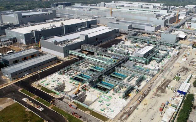
Against this backdrop, one of the main drivers behind the equipment sale is the ongoing process upgrade at the Xi’an fab. According to Global Economic, the facility contributes around 40% of Samsung’s total NAND output and remains a key strategic base, helping sustain supply chain stability even amid U.S.-China semiconductor tensions.
As part of this transition, Samsung has discontinued production of its 128-layer V6 NAND at Xi’an and is now focusing on its 236-layer V8 generation in mass production. The company plans to introduce 286-layer V9 NAND in 2026, with a longer-term roadmap targeting more than 400 layers. Global Economic adds that this strategy is aimed at shifting competition toward the premium segment above 200 layers, where technological barriers are higher.
Global Economic also notes that the rapid buildout of AI infrastructure is driving strong demand for enterprise-grade, high-performance SSDs, underscoring the growing importance of high-density, low-power NAND. This trend is further accelerating Samsung’s shift away from legacy processes.
Profitability Gains in Focus, but Risks Remain
Market analysts expect Samsung to ease oversupply and boost profitability by phasing out older processes. However, Global Economic notes that several risks remain. First, demand cycle uncertainty: if AI demand peaks earlier than expected, the risk of excess capacity could increase. Second, technological complexity: as layer counts exceed 300, manufacturing becomes significantly more complex, making it harder to achieve stable yields in the early stages—an issue that could directly affect profitability. The report also highlights geopolitical uncertainty, noting that U.S. export controls on advanced equipment to China could impact the execution of the Xi’an fab’s roadmap.
Read more
- [News] Samsung Reportedly Advances Xi’an to 236-Layer NAND; SK hynix Eyes Dalian Upgrade Amid Tight Supply
- [News] Samsung Reportedly Ends Last 2D NAND Line as Early as March, Repurposes Facility for 1C DRAM
(Photo credit: Samsung)


