[News] NVIDIA’s Rubin Ultra Seen Sticking to Dual-Die Design on Packaging Constraints; TSMC 3nm Demand Intact
As NVIDIA’s Rubin moves into mass production, industry attention is already shifting to the specifications of its next-generation Rubin Ultra. While market rumors suggest that Team Green may integrate four GPU dies and 16 HBM4E stacks within a single package, Commercial Times indicates that current foundry planning remains focused on a dual-die (2-die) architecture, with TSMC’s overall wafer start volumes staying intact.
Commercial Times notes that Rubin Ultra is slated for launch in 2027, continuing a chiplet-based design on TSMC’s N3P process with CoWoS-L advanced packaging. Sources cited by the report further indicate that NVIDIA has fine-tuned its wafer-start allocation, shifting more capacity toward the Blackwell generation rather than cutting orders.
Against this backdrop, demand for TSMC’s 3nm node is expected to stay robust. With capacity still tight and hyperscaler demand for in-house AI chips holding firm, NVIDIA has limited incentive to scale back wafer starts, as doing so could risk weakening its position in the AI server market, the report notes.
Notably, Next Apple, citing TrendForce, highlights that AI is set to claim 36% of 3nm capacity in 2026, up from just 5% in 2025—and potentially more—creating a pronounced crowding-out effect. Major in-house chips from hyperscalers, including Google TPU v7 and Google TPU v8, as well as AWS Trainium v3, are expected to be produced on TSMC’s 3nm node.
According to Commercial Times, NVIDIA’s decision not to adopt a four-die, single-package design for Rubin Ultra reflects mounting constraints in advanced packaging. A 4-die configuration would expand the package size to roughly 7.5–8 times the reticle limit, significantly weighing on yield and cost, the report explains. As a result, the design is now trending toward a dual-die architecture, prioritizing manufacturing efficiency and mass-production viability.
Read more
- [News] NVIDIA Rubin Ultra and Feynman Reportedly to Boost TSMC SoIC; Besi, Applied Materials, TEL to Benefit
- [News] Key GTC Takeaways: How Samsung, Micron, Intel & More Power NVIDIA’s Vera Rubin and Feynman
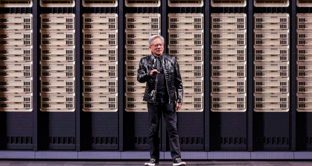
(Photo credit: NVIDIA)


