[News] ASML Reportedly Eyes Hybrid Bonding Equipment, Precision Edge May Reshape Advanced Packaging Landscape
Rumors have recently resurfaced that lithography leader ASML is evaluating entry into the back-end semiconductor equipment market, targeting the fast-growing advanced packaging segment. According to Korean media outlet The Elec, ASML has begun developing hybrid bonding equipment—widely regarded as a key technology for next-generation chip packaging.
Sources indicate that ASML has initiated the architectural design of hybrid bonding systems for back-end processes and has recently engaged external partners for system development.
Potential collaborators include Prodrive Technologies and VDL-ETG, both long-standing suppliers within ASML’s ecosystem. Prodrive provides linear motors and servo drives for the magnetic levitation (maglev) systems used in ASML’s EUV lithography platforms, while VDL-ETG is responsible for manufacturing key mechanical structures.
Maglev systems enable ultra-precise wafer stage motion with significantly lower vibration compared to conventional air-bearing systems. As hybrid bonding processes demand extremely high alignment accuracy between dies and wafers, such precision motion technologies are increasingly being adopted to improve yield and performance.
Hybrid bonding is emerging as a critical enabler for advanced packaging. Unlike traditional thermocompression (TC) bonding, which relies on micro-bumps, hybrid bonding directly connects copper surfaces between chips, enabling higher interconnect density and lower resistance. The process requires equipment capable of die pick-up, ultra-precise alignment, and pressure-assisted bonding—placing stringent demands on system accuracy and stability.
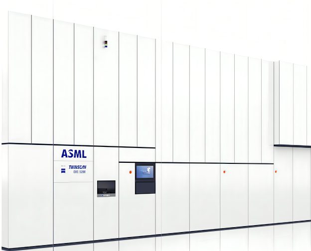
Industry sources note that ASML’s move into hybrid bonding is not unexpected. As early as 2024, the company introduced its first back-end system, the TWINSCAN XT:260 3D DUV lithography tool, designed for advanced packaging applications such as redistribution layer (RDL) patterning on interposers. ASML has also proposed integrated lithography solutions combining DUV and EUV scanners, achieving wafer bonding overlay accuracy of around 5 nm—laying the groundwork for further expansion into high-precision packaging processes.
ASML Chief Technology Officer Marco Peters has previously stated that the company is closely evaluating opportunities in semiconductor packaging and assessing how to build a relevant product portfolio. Following a review of technology roadmaps from memory manufacturers including SK hynix, ASML has reportedly confirmed clear demand for advanced stacking process equipment.
On the market side, the rapid growth of advanced packaging is another key driver. Equipment supplier Besi reported a 105% year-over-year increase in backlog in the fourth quarter, largely driven by hybrid bonding demand. Meanwhile, ASMPT estimated that advanced packaging would contribute approximately 25% of its total revenue.
Also, Applied Materials has already entered this field, partnering with Besi to develop the Kynex die-to-wafer (D2W) hybrid bonding system, integrating Besi’s Datacon 8800 Cameo Ultra Plus AC platform to strengthen its competitive position.
Another industry insider points out that ASML possesses some of the world’s most advanced ultra-precision control technologies. Should its hybrid bonding systems materialize, they could significantly reshape the current competitive landscape. However, ASML has stated that it has not yet officially kicked-start any hybrid bonding business.
(Photo credit: ASML)


