[News] China Achieves 14-Inch SiC Breakthrough, Intensifying Global Large-Wafer Competition
On March 11, Tiancheng Semiconductor announced that it had successfully developed a 14-inch silicon carbide (SiC) single crystal using self-developed equipment, with an effective thickness of 30 mm. The breakthrough marks China’s transition in large-sized SiC materials—from the “12-inch adoption phase” to the first step toward 14-inch commercialization.
Recently, a number of companies worldwide have stepped up efforts in 12-inch and 14-inch SiC single crystals and substrates, creating a diversified competitive landscape. Behind this global race toward larger wafer sizes lies the core industry goal of reducing costs, improving efficiency, and capturing high-end markets in the wide bandgap semiconductor sector.
Compared with the current mainstream 6-inch and 8-inch SiC substrates, 12-inch and larger wafers significantly increase the effective chip area under the same production conditions. This not only lowers the manufacturing cost per chip but also better supports high-end applications such as power devices and semiconductor equipment components. Larger wafers are therefore expected to play a crucial role in the technological upgrades of sectors including electric vehicles, photovoltaic energy storage, and AI data centers.
Industry estimates suggest that 12-inch SiC substrates can deliver more than three times the chip output per unit area compared with 6-inch wafers, while reducing overall costs by roughly 40%. The introduction of 14-inch wafers could further amplify these advantages, pushing SiC toward a new stage of large-scale industrial adoption.
Global Competition in Large-Sized SiC Accelerates
In the 12-inch segment, leading Chinese companies and emerging players are advancing in parallel, forming a diversified competitive landscape:
- San’an Optoelectronics: 12-inch SiC substrates have been delivered to customers for validation.
- SemiSiC: Developer of the world’s first 12-inch high-purity semi-insulating SiC single-crystal substrate, currently advancing a project aimed at annual production of one million SiC substrates.
- Roshow: Announced in February 2026 that it had produced its first 12-inch SiC single-crystal sample.
- HiMahines (Hymson’s subsidiary): Successfully developed a 12-inch SiC single-crystal ingot.
- JSG (Jingsheng): Achieved a breakthrough in 12-inch conductive SiC single-crystal growth in May 2025. By September the same year, its 12-inch pilot line had come online with 100% domestically produced core equipment, and in January 2026 it reached a key technical milestone with substrate thickness uniformity (TTV) ≤ 1 μm.
Globally, the “wafer-size race” in SiC is heating up, with international players also pushing forward:
- Wolfspeed: In January 2026, it announced the manufacture of a 300 mm (12-inch) SiC single-crystal wafer. Its 300 mm platform is designed to support both power device manufacturing and high-purity semi-insulating substrate development.
- SK Siltron: Its SiC wafer fab in Bay City, Michigan, has entered operation with an expected annual capacity of 60,000 wafers, primarily focused on 8-inch mass production, while 12-inch development remains underway.
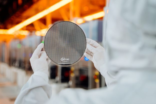
- Infineon: Has launched a SiC wafer fab in Malaysia, which could become the world’s largest 200 mm (8-inch) SiC power semiconductor wafer facility.
- STMicroelectronics: Is expanding its 8-inch SiC device manufacturing through a joint venture with San’an.
(Photo Credit: Infineon)


