[News] Samsung and NVIDIA Team Up on Ferroelectric NAND R&D, Key Step Toward 1000-Layer NAND
NVIDIA and Samsung are taking their partnership beyond HBM for GPUs. On March 6, researchers from Samsung Semiconductor Research, NVIDIA, and Georgia Tech unveiled the PINO (Physics-Informed Neural Operator) AI model, capable of analyzing ferroelectric NAND performance 10,000× faster than traditional methods, supercharging next-gen memory R&D, Sedaily reports.
Ferroelectric NAND, capable of 1,000 stacked layers and slashing power consumption by up to 96%, is emerging as a next-gen solution to tackle both supply shortages and energy demands, Sedaily explains. Its game-changing potential may explain why NVIDIA—a company known for GPUs—has taken the unusual step of joining R&D for a future, not-yet-commercialized memory technology, according to the report.
What is Ferroelectric NAND?
The report points out that ferroelectric materials can maintain polarized states without high external voltage, allowing electrons to move between positive and negative poles to store digital 0s and 1s, while traditional silicon requires higher voltage. Replacing silicon with ferroelectric materials could drastically reduce power consumption.
The material’s potential has Samsung stepping up related development efforts. According to the Intellectual Property Office data cited by Sedaily, Samsung leads global ferroelectric patents with a 27.8% share, ahead of Intel, TSMC, and SK hynix.
However, as commercializing ferroelectric NAND requires analyzing the material’s complex properties and optimizing device structures, Samsung and NVIDIA now jointly introduced an AI tool that can analyze performance 10,000× faster than conventional methods. According to Sedaily, traditional TCAD simulations, commonly used in the industry, can take around 60 hours per run, whereas the new AI cuts this to under 10 seconds.
Paving Way for 1000-layer NAND
As the report highlights, Samsung’s NAND stacking currently reaches 200–300 layers, with ferroelectric technology seen as the key to scaling up to 1,000 layers.
For now, Samsung is reportedly targeting a 2030 roadmap for 1,000-layer NAND. According to The Bell, the company revealed a product architecture for this next-gen NAND in late February at the International Solid-State Circuits Conference (ISSCC).
Notably, this design could be regarded an upgraded version of the Bonding Vertical (BV) NAND, stacking 4 wafers—2 cell wafers atop 2 peripheral wafers—to overcome previous structural limits, the report notes, adding that Kioxia is also conducting research under the name Multi-Stack CBA (CMOS directly Bonded to Array).
Read more
- [News] Samsung Reportedly Ends Last 2D NAND Line as Early as March, Repurposes Facility for 1C DRAM
- [News] Samsung Readies New Price Hikes: Consumer DRAM, SSD Reportedly Doubled, NAND Set for 50%+ Rise
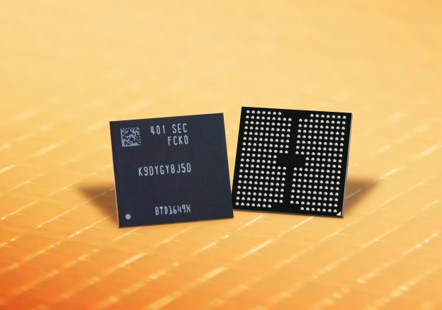
(Photo credit: Samsung)


