[News] Samsung Reportedly Secures Partial Taylor Fab Use Approval, Timeline May Move Up
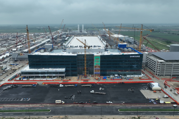
Samsung’ Taylor fab is reportedly making tangible progress. Citing Korea JoongAng Daily, the report says the company has obtained temporary approval for portions of its facility under construction in Taylor, potentially accelerating the project from its original schedule.
As noted in the report, a Taylor city official said on the 5th that Samsung Electronics has secured a Temporary Certificate of Occupancy (TCO) for parts of its first fab, covering about 88,000 square feet (roughly 8,175 square meters). The report adds that TCOs are being issued section by section, and while further approvals are expected, no firm timeline has been set.
Additional signs of progress have also emerged. According to the report, South Korean chip equipment and services firm Device disclosed on the 29th that it had won a KRW 10.9 billion contract from Samsung’s U.S. unit to supply semiconductor cleaning equipment. Deliveries are scheduled to be completed by October, and industry sources say the tools are highly likely to be installed at the Taylor fab.
Sources cited by the report add that Samsung is likely to begin testing extreme ultraviolet (EUV) lithography tools as early as next month. These tests would mark a key milestone toward mass production of 2nm chips, with full-scale output targeted for the second half of 2026. Once mass production ramps up, the report says the Taylor plant will manufacture Tesla’s AI5 chips under a contract running through 2033, and is also expected to supply the company’s next-generation AI6 chips.
Samsung Reportedly Invests in ASML-Alumni Metrology Firm to Boost 2nm Yield Stability
Alongside efforts to speed up its Taylor fab timeline, Samsung is also seeking to improve 2nm yields by investing in equipment-related companies. According to Hankyung, sources say Samsung Electronics acquired a minority stake late last year in Invisix through its investment arm, Samsung Venture Investment. Founded by former ASML employees, Invisix is expected to become a key partner in validating the performance of the EUV lithography tools.
Invisix’s technology can address the limitations of existing metrology tools, which can be either too slow or overly sensitive when detecting defects. If applied to Samsung’s 2nm GAA process—a node the company is heavily betting on—it is expected to deliver meaningful synergies in stabilizing yields, Hankyung notes.
Samsung Foundry Eyes New Clients Beyond Tesla
Looking ahead, Samsung’s foundry business is said to be seeking additional customers beyond Tesla, with Google and AMD often cited as potential candidates. After several years of losses, Samsung Foundry is expected to return to profitability this year as Tesla-related volumes ramp up, with the business targeting double-digit year-on-year revenue growth, Korea JoongAng Daily adds.
According to ZDNet, Samsung Electronics said progress on its 2nm node, along with related customer order intake, is proceeding smoothly. The report notes that the company says that following the Tesla order, it is in talks with major U.S. and Chinese customers and expects the number of 2nm-related order to rise by more than 30% year on year this year.
Read more
- [News] Samsung Set to Benefit from TSMC’s ‘N-2’ Rule as AMD, Google Eye U.S. 2nm Production
- [News] Samsung Foundry Reportedly Expects 30%+ 2nm Order Growth in 2026; 1.4nm Set for 2029
(Photo credit: Samsung)
Please note that this article cites information from Korea JoongAng Daily, Hankyung, and ZDNet.


