[News] Samsung Accelerates Taylor Fab Ramp-Up, Domestic EUV Pellicles Reportedly Enter U.S. Line
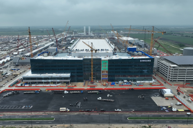
Samsung is accelerating the ramp-up of its Taylor fab, with trial runs of extreme ultraviolet (EUV) lithography tools reportedly beginning as early as March. Adding to the momentum, ETNews reports that the company has awarded a KRW 25 billion contract to South Korean supplier FST for EUV pellicle handling equipment at the U.S. site—marking the key usage of domestically sourced pellicle solutions in its American operations.
Notably, ETNews notes that foundry leader TSMC started introducing metal silicide EUV pellicles from Japan’s Mitsui Chemicals back in 2019. Samsung, in contrast, has focused on domesticizing the technology, investing in S&S Tech and FST in 2020 and 2021, respectively, the report adds.
As highlighted by the report, Samsung currently operates more than 70 EUV lithography tools, the second-largest installed base globally after TSMC. As a result, the introduction of domestically developed EUV pellicles is expected to have a significant ripple effect across the equipment and components supply chain. EUV pellicle prices are estimated to exceed KRW 60 million per unit, the report suggests.
In comparison, The Elec previously reported that conventional DUV pellicles—such as ArF and KrF—typically sell for a few hundred thousand won per unit, with the priciest models around KRW 1 million won.
According to ETNews, the tools supplied by FST support not only next-generation carbon nanotube (CNT) EUV pellicles but also conventional metal silicide (MeSi) EUV pellicles.
Samsung Speeds up Taylor Progress
According to Munhwa IIbo, Samsung is raising the process node of its Taylor fab from the originally planned 4nm to 2nm. As noted by the report, the scale of production is striking: while industry estimates initially pegged 2nm output at around 20,000 wafers per month, Samsung now expects the Taylor fab to exceed 50,000 wafers monthly—more than double earlier projections and on par with TSMC’s planned 2nm ramp in Taiwan.
Meanwhile, Hankyung reports that trial operations of extreme ultraviolet (EUV) lithography equipment at Taylor Fab 1 will start this March, setting the stage for mass production of Tesla’s AI5 and AI6 autonomous driving chips. As per Hankyung, Samsung plans to sequentially install etching and deposition tools, with full-scale production scheduled for the second half of 2026.
Read more
- [News] Samsung Reportedly Sets March EUV Trials at Taylor Fab Ahead of Tesla Chip Production
- [News] Samsung Chairman Reportedly Meets Musk, Granting Tesla CEO Dedicated Workspace at Taylor Fab
(Photo credit: Samsung)
Please note that this article cites information from ETNews, The Elec, Munhwa IIbo and Hankyung.


