[News] SK hynix to Build Cheongju Advanced Packaging Fab, Boosting HBM Output by 2027
As previously reported by ZDNet, SK hynix is exploring plans for its first U.S. HBM packaging facility. Meanwhile, the memory giant is accelerating its domestic expansion, announcing today a KRW 19 trillion investment in a new advanced packaging fab, P&T7, at its Cheongju site. The facility is poised to become a key hub for AI memory production, including HBM.
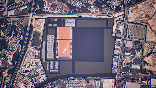
According to SK hynix’s press release, situated on a 70,000-pyeong (approx. 231,400 m²) site within the Cheongju Technopolis Industrial Complex, construction is set to begin in April 2026, with full operations expected by the end of 2027. The Chosun Daily further points out that this move positions the company with three strategic packaging hubs: Icheon in Gyeonggi Province, Cheongju in the non-capital region, and West Lafayette, Indiana in the U.S.
SK hynix is betting on rapid HBM growth, projected to hit a 33% CAGR between 2025 and 2030, by ramping up production across its Cheongju fabs. Following the M15 fab in 2018 and the KRW 20 trillion M15X project announced in 2024, the company said it is moving ahead of schedule: the M15X cleanroom opened in October 2025, and equipment is now being installed sequentially.
According to The Elec, SK hynix plans to start 1b DRAM production for the latest HBM4 at M15X in February, four months earlier than initially planned. Initial output is expected at ~10,000 wafers per month, with capacity set to expand multiple times by the end of 2026, the report adds.
As the Chosun Daily explains, Cheongju is already home to SK hynix’s M11, M12, and M15 fabs, which produce NAND, alongside P&T3, a facility handling back-end processes. The ongoing M15X project, together with the newly announced P&T7 fab, is expected to cement Cheongju as SK hynix’s central hub for AI memory production, the report highlights.
The Elec notes that the P&T fab packages semiconductor chips produced at front-end fabs and verifies their quality before integration into final products. Using 2.5D packaging, which stacks chips vertically and incorporates through-silicon vias (TSVs) in DRAM, the fab can manufacture HBM.
Meanwhile, The Financial News previously highlighted Samsung Electronics’ Cheonan campus as the company’s advanced packaging powerhouse.
Read more
- [News] SK hynix 2026 Outlook: HBM3E Dominates, HBM4 Dual Strategy Amid 3 Market Headwinds
- [News] SK hynix Reportedly Plans First U.S. 2.5D Packaging Line, Eyes Turnkey HBM to Challenge TSMC
(Photo credit: SK hynix)
Please note that this article cites information from SK hynix, The Chosun Daily, The Elec, ZDNet and The Financial News.


