[News] Intel Eyes EMIB to Ramp up in 2H26; 18A‑P/18A‑PT Moves Toward External Adoption

As interest around Intel’s EMIB (Embedded Multi-die Interconnect Bridge) continues to build—including reports linking it to a Google-MediaTek TPU—the industry is watching closely for signs of a real ramp. According to Intel’s Corporate Vice President John Pitzer, the technology is expected to begin making a meaningful contribution as it ramps more noticeably in the second half of 2026.
According to Intel’s UBS Global Technology and AI Conference 2025 transcript on Seeking Alpha, initial demand spiked due to a CoWoS shortage. However, Pitzer noted that as Intel showcased its EMIB and EMIB-T roadmap, client interest grew, with EMIB seen as offering capabilities beyond CoWoS. The focus has thus shifted from overflow demand to technology-driven adoption, he added.
Indeed, Intel is accelerating its push in advanced packaging recently. ETNews says it has established its EMIB process at Amkor’s Songdo K5 facility in South Korea, marking its first-ever outsourcing of high-end packaging. Meanwhile, TechPowerUp reports Intel is finalizing its $7 billion “Project Pelican” complex in Malaysia, which will handle both EMIB and Foveros.
According to TrendForce, the company has successfully implemented this technology in its own server CPU platforms, including Sapphire Rapids and Granite Rapids. As Google plans to implement EMIB in its 2027 TPU v9 and Meta considers it for its MTIA accelerators, EMIB is set to significantly boost IFS’s growth.
Opens 18A-P/18A-PT to External Clients
Pitzer highlighted for now, yields for 18A aren’t yet “optimal,” but have improved remarkably since CEO Lip-Bu Tan took charge in March, according to Wccftech. TechPowerUp notes with Panther Lake on schedule, Pitzer said that if monthly 7% yield gains continue, Intel could reach full-volume production without major per-unit cost increases.
Pitzer further noted that while 18A is going to be mostly an internal node, 18A-P will be used both for the internal customer and external customers as well. It is worth noting that he also emphasized that 18A-PT will serve as the base die for advanced packaging and will be used for both Intel’s own products and for external customers.
Notably, as per the transcript, Intel expects about 70% of the logic compute tiles for Panther Lake to be produced internally—compared with 0% for Arrow Lake and Lunar Lake. The share will improve further with Nova Lake, which extends the strategy to desktop parts. By the end of 2026 and into 2027, Intel will also benefit from bringing desktop wafers back in-house, expanding internal production beyond notebooks, as noted in the transcript.
More Colors on 14A
Regarding 14A progress, Intel noted in the transcript that it has engaged external customers in the definitional phase. As the key question is when Intel will secure external customers for 14A or 18AP, fabless customers are expected to make firm decisions on 14A designs between the second half of 2026 and the first half of 2027, according to Pitzer.
As Intel’s 14A node is a second-generation gate-all-around technology with second-generation backside power, the node could build on lessons from 18A, according to Pitzer. While 18A pushed physics in new ways, 14A is already showing meaningful lead in yield and performance compared with 18A at a similar stage, offering a promising outlook, he added.
Read more
- [News] Intel Reportedly Taps Amkor’s Songdo Facility for EMIB Packaging in First-Ever Outsourcing Move
- [News] Intel Gains Momentum: 18A Eyes Apple, EMIB Reportedly Tapped for Google-MediaTek TPUs
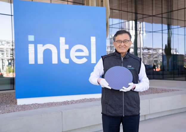
(Photo credit: Intel)


