[News] TSMC, Samsung Reportedly Cut 8-Inch Wafer Output, Boosting Korea’s DB HiTek
Samsung and TSMC are reportedly scaling back their 200mm (8-inch) foundry operations in response to shifting industry dynamics. According to South Korean outlet Hankyung, the two chipmakers have recently begun focusing more on advanced manufacturing using 300mm (12-inch) wafers to produce high value-added processors such as GPUs.
The report, citing industry sources, states that TSMC plans to cut about 30% of its 200mm production lines over the long term, while Samsung has already scaled its 200mm capacity down to roughly half of its peak and is considering additional reductions. Still, both companies continue to serve clients dependent on 200mm foundry lines and are not planning a complete exit from the segment.
DB HiTek Gains Momentum as Samsung and TSMC Scale Back 200mm Lines
This shift has created a major opportunity for DB HiTek, Korea’s second-largest foundry, whose main operations remain centered on the 200mm segment. The downsizing of Samsung and TSMC’s 200mm businesses has had a direct positive impact on DB HiTek’s performance. The report notes that tighter supply of 200mm wafers has lifted the company’s fab utilization rates, with product prices also expected to rise.
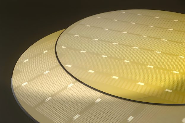
DB HiTek specializes in 200mm wafer fabrication, producing legacy chips such as display driver ICs (DDIs) for TVs and power management ICs (PMICs) that regulate electrical power in electronic devices. This segment remains central to the company’s operations, supported by steady demand across industries that continue to rely on mature process technologies, according to the report.
Rising demand for power semiconductors has become a key growth driver for DB HiTek, lifting its third-quarter operating profit 71% year-on-year to 47.1 billion won ($32 million), the report notes. Building on this momentum, the company plans to begin full-scale foundry production of next-generation power semiconductors—such as silicon carbide (SiC) and gallium nitride (GaN)—using 200mm wafers in the fourth quarter of next year.
Samsung and TSMC Pivot to 300mm as Chinese Competition Intensifies
Meanwhile, Samsung and TSMC are redirecting resources toward 300mm manufacturing. Growing price pressure from Chinese foundries is another factor behind the reduction in 200mm operations for Samsung and TSMC. Chinese manufacturers using 70–180 nm processes have lowered wafer prices to around $2,500 each, intensifying competition in the low-cost market. The report also points out that for major foundries like Samsung and TSMC, focusing on 300mm production, where a single 3nm wafer can yield chips worth up to $20,000, is a more pragmatic business decision.
Read more
- [News] TSMC Reportedly Phases Out Legacy Production, Closing 6-Inch Fab 2 and 8-Inch Fab 5 by 2027
- [News] South Korea Launches First 8-Inch SiC Plant in Busan, Annual Output Projected at 30K Wafers
(Photo credit: DB HiTek)
Please note that this article cites information from Hankyung.


