[News] SK hynix Reportedly Explores High-Bandwidth Storage Stacking NAND and DRAM
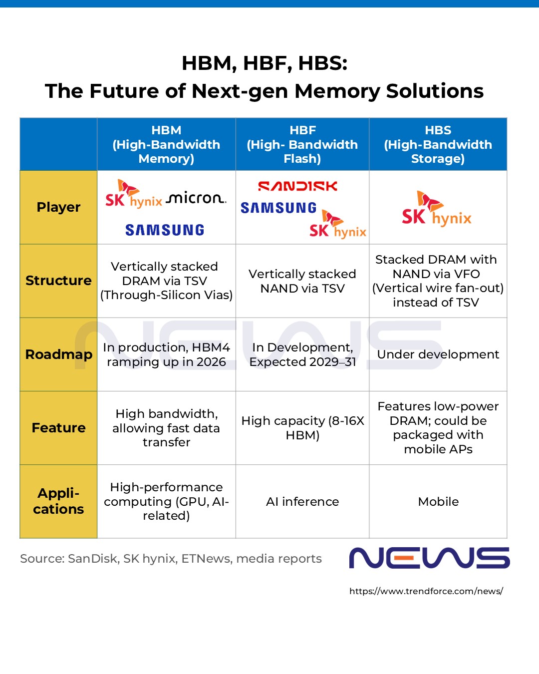
After solidifying its leadership in HBM, SK hynix is teaming up with SanDisk to develop High-Bandwidth NAND Flash (HBF), which enhances HBM with NAND for AI inference workloads. At the same time, the company is reportedly exploring a broader memory spectrum: High-Bandwidth Storage (HBS). As ETnews reports, HBS combines mobile DRAM and NAND to boost AI performance in smartphones, tablets, and other mobile devices.
Sources cited in the report explain that SK hynix is stacking low-power Wide I/O DRAM with NAND to create HBS, which can stack up to 16 layers of DRAM and NAND. These layers are interconnected via vertical wire fan-out (VFO), significantly enhancing data processing speeds, as per ETNews.
Notably, this is not SK hynix’s first use of VFO. ETNews reports that the company previously supplied DRAM packaged with vertical wire fan-out technology for Apple’s Vision Pro, and the new HBS pushes the concept further by integrating NAND.
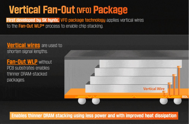
According to SK hynix, VFO, debuted in 2023, is a technology that minimizes space and reduces power consumption by connecting wires vertically instead of curving them. It has also revolutionized the sizeable fan-out wafer-level package (WLP), a packaging technology which connects I/O terminals with wires from the outside of the chip.
SK hynix claims its Vertical Fan-Out design delivers significant gains: wire lengths are reduced by 4.6 times compared to conventional designs, translating to a 4.9% bump in power efficiency. Beyond that, the technology shaves 27% off packaging height and improves heat dissipation by 1.4%, the company notes.
It is worth noting that unlike HBM, HBS does not require through-silicon via (TSV) processes that penetrate the chip, giving it higher yields and lower manufacturing costs, the report points out.
Potential Applications/ HBF Roadmap
Looking ahead, ETNews notes that the DRAM-and-NAND stacked HBS is packaged with the application processor (AP) and integrated directly into mobile devices. Thus, the report suggests that SK hynix developed HBS to meet the rising demand for enhanced AI performance in smartphones, tablets, and other mobile platforms.
SK hynix’s latest move aligns with its earlier patent filing. As reported by Sisa Journal in March, the company applied for the “LPW NAND” trademark with the Korean Intellectual Property Office (KIPO) in February—a technology believed to mirror SanDisk’s High-Bandwidth Flash (HBF). SanDisk’s first-generation HBF stacks 16 layers to reach 512GB, delivering HBM-like bandwidth while expanding capacity 8–16 times, the report noted.
Looking ahead, SK hynix’s HBF product is projected to arrive between 2029 and 2031, according to a roadmap cited by Wccftech.
Read more
- [News] Memory Giants SanDisk, SK hynix Unite for HBF Standard, with Samples Expected in 2H26
- [News] Kioxia Reportedly Eyes 2027 Launch for NVIDIA-Partnered AI SSDs with 100x Speed Boost
(Photo credit: SK hynix)
Please note that this article cites information from ETnews, Sisa Journal, Wccftech and SK hynix.


