[News] Amkor Breaks Ground on USD 7 Billion Advanced Semiconductor Packaging Facility in Arizona
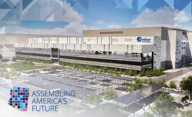
Chip packaging and testing giant Amkor Technology has officially broken ground on its new advanced packaging campus in Peoria, Arizona, marking a major expansion of its U.S. manufacturing footprint.
Amkor initially planned to invest USD 2 billion to build a packaging and testing plant in the Five North at Vistancia community of Peoria. However, in late August, the company announced a revised site plan — relocating the project to Peoria Innovation Core in northern Peoria and expanding the land area from 56 acres to 104 acres.
According to the latest update, Amkor will inject an additional USD 5 billion, bringing the total investment to USD 7 billion. The expanded plan includes new cleanroom facilities and the construction of a second packaging and testing factory.
Amkor emphasized that the new campus, strategically located in Arizona’s high-tech corridor, will become the most advanced outsourced semiconductor packaging and testing hub in the United States. It will focus on state-of-the-art packaging and testing technologies designed to complement TSMC’s wafer fabrication capabilities, meeting the evolving demands of AI, high-performance computing (HPC), mobile communications, and automotive applications.
The project will be executed in two phases. Upon completion, the campus will feature over 750,000 square feet of cleanroom space and create up to 3,000 high-quality jobs. The first manufacturing facility is scheduled for completion in mid-2027 and volume production in early 2028. These new facilities are expected to serve as a cornerstone of America’s advanced packaging capacity, supporting key customers including Apple and NVIDIA.
As AI accelerator, HBM memory, and multi-die architecture rapidly gain traction, advanced packaging has become a critical step in chip manufacturing. The U.S. National Institute of Standards and Technology (NIST) has noted that shortages in 2.5D packaging capacity have emerged as a major bottleneck for AI chip mass production, delaying shipments of several GPUs.
Amkor stated that its Arizona campus will specialize in high-density integration and high-frequency interconnect packaging technologies, supporting localized production of AI and HPC chips. The company will also collaborate with local universities and technical training institutions to cultivate a skilled semiconductor workforce for the region.
(Photo credit: Amkor’s X)


