[News] Intel to Unveil 18A at Tech Tour: Reportedly Limited Q3 Shipments, Panther Lake Debuts Oct. 9

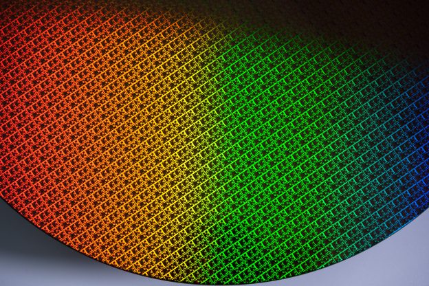
With Team Blue currently hosting its first Intel Tech Tour in Arizona, new details on the 18A ramp-up have emerged. Commercial Times reports that the semiconductor began limited shipments to U.S. customers in Q3, with 18A wafers already in production and initial output of its own CPUs expected in Q4.
Notably, TweakTown reveals that Intel will unveil its first in-house 18A processor, Panther Lake, on October 9, during the tour. The Economic Daily News notes that the Panther Lake AI PC chip is slated to ship by year-end, with the 18A rollout set to underpin Intel’s next three generations of CPUs.
Implication of 18A Production at Arizona
As per Commercial Times, Intel, by kicking off 18A mass production, has become the first among foundry rivals to introduce backside power delivery. Most notably, with 18A starting production in Arizona, the site will become the first in the U.S. to enter 2nm-class mass production, the report highlights.
Intel’s Arizona expansion—Fab 52 and Fab 62—is part of a $32 billion investment launched in 2021. Fab 52 alone is expected to reach 1,000–5,000 wafers per month by year-end, ramp to 15,000 in 2026, and ultimately hit 30,000, according to Commercial Times.
Industry sources cited by Commercial Times note that, alongside U.S. chip tariff policies, Intel’s Arizona fabs are set to become a key option for chipmakers. While 18A still lags in transistor density, its backside power delivery reduces routing congestion and boosts frequency performance, drawing interest from global tech giants, the report adds.
On the other hand, the Economic Daily News highlights that Intel and TSMC’s fabs are located north and south of Phoenix, solidifying the region as a U.S. semiconductor hub.
According to the report, TSMC’s first Arizona fab kicked off 4nm production in Q4 2024. The company previously noted that Fab 2 is completed and will feature 3nm, with efforts underway to accelerate its ramp-up by several quarters. The Economic Daily News suggests that TSMC may be moving even faster, with Fab 3, featuring 2nm and A16, potentially entering mass production as early as 2027—one year ahead of the original schedule.
Spotlight on 18A
For more technological details on the node, Intel previously noted that 18A, the company’s most important transistor innovation since it introduced FinFET (fin field-effect transistor) to high-volume manufacturing in 2011, integrates its new PowerVia backside power, which shifts thick metal layers and bumps to the back of the die, and RibbonFET gate-all-around (GAA) technologies to significantly improve performance per-watt and density.
Compared with Intel 3, the 18A process reportedly delivers a 15% improvement in performance per watt and a 30% increase in chip density.
By contrast, the Economic Daily News notes that TSMC plans to implement its own backside power solution, Super Power Rail (SPR), with the next-generation A16 process.
Intel’s server CPU, Clearwater Forest, will also be built on 18A and is slated for the first half of 2026, which also marks the introduction of the company’s next-gen Foveros Direct 3D advanced packaging technology, as per the Economic Daily News.
According to Commercial Times, in advanced packaging, Intel is betting on two flagship technologies: Foveros (3D stacking) and EMIB (Embedded Multi-die Interconnect Bridge). Commercial Times explains that EMIB uses embedded silicon bridges at die edges instead of a full interposer, offering greater packaging flexibility and lower cost compared with large-area CoWoS solutions.
Read more
- [News] Intel Rumored to Build Tesla Chips on 18A; Gaudi 3 Sees Early Momentum in Dell Servers
- [News] Intel’s Clearwater Forest Unveils 18A Backside Power at Hot Chips; TSMC’s Super Power Rail to Follow
(Photo credit: Intel)


