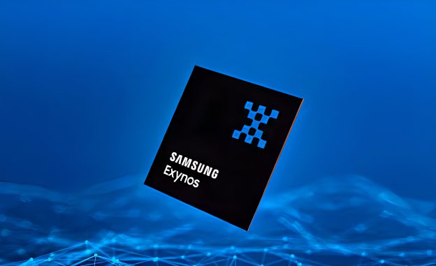
[News] Samsung Reportedly Starts Exynos 2600 Mass Production, Yield Estimated to Reach 50%

According to South Korean outlet The Bell, Samsung has reportedly begun mass production of its next-generation application processor, the Exynos 2600, ahead of expectations—the company’s first chip built on the SF2 (first-generation 2nm) process.
As the report notes, a key reason Samsung began Exynos production in September was the quicker-than-expected improvement in yields. The SF2 process yield climbed from around 30% in Q1 to an estimated 50%. Still, this number reflects an AP benchmark, with real yields varying by die size.
Sources on the 29th said Samsung has recently begun wafer input for Exynos 2600 production. The “fab out”—when a wafer completes front-end processing and leaves the fabrication line—is expected between late October and early November, as the report highlights. The report adds that after fab-out, the chips will move on to wafer testing, packaging, and final inspection. Wafer testing is outsourced to partners, while packaging and subsequent testing are carried out internally by Samsung.
The report notes that with Exynos 2600 entering production, its inclusion in the Galaxy S26 is now almost certain. While the processor allocation has not been officially confirmed, past patterns reportedly suggest Exynos for domestic and European models and Snapdragon for North America and China.
Samsung’s 2nm Push
Samsung’s reported yield gains on the Exynos 2600 could strengthen its foothold in advanced foundry markets if the project succeeds. Notably, to compete with TSMC, the company has reportedly cut its 2nm wafer price to $20,000—a 33% discount from TSMC’s expected $30,000 rate, according to TechPowerUp. The move aims to utilize idle foundry capacity as Samsung faces pressure to recoup massive investments in next-generation fabrication in South Korea and the U.S., the report adds.
Meanwhile, Samsung’s 2nm has already begun drawing major customers, with The Bell highlighting that Tesla has signed a USD 16.5 billion foundry agreement to produce its “AI6” system chip on the SF2P (second-generation 2nm) process. The report also notes that Japanese AI unicorns like Preferred Networks (PFN) and Ambarella, along with AD Technology, are developing chips using Samsung’s 2nm technology.
As noted by The Bell, SF2 represents Samsung’s most advanced process node to date, built on third-generation gate-all-around (GAA) technology. Compared with SF3, it delivers roughly a 12% performance boost and a 25% improvement in power efficiency.
Read more
- [News] Qualcomm Launches Snapdragon 8 Elite Gen 5, May Plan Samsung Galaxy-Exclusive Version
- [News] Samsung Reportedly Secures Foundry Deal for IBM Power11 Using 7LPP EUV Process
(Photo credit: Samsung)


