[News] Samsung Reportedly Shifts Cheonan Capacity to HBM Packaging, Outsource Conventional Memory Modules
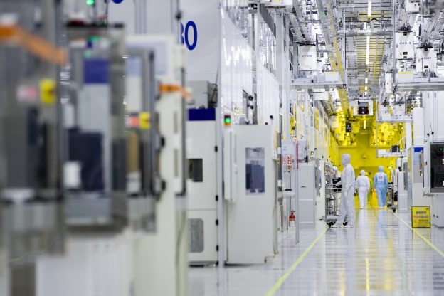
Samsung Electronics is reportedly reshaping its back-end operations in Cheonan as rising HBM demand drives a shift in packaging capacity. According to Sisa Journal, sources say the company plans to gradually phase out Exynos mobile application processor (AP) packaging at the site and convert the related equipment for HBM packaging. The transition is reportedly set to begin next year.
Cheonan will continue handling existing products, including the Exynos 2600 used in some Galaxy S26 series models and the Galaxy Z Flip 8, but dedicated packaging lines for future Exynos products are not planned at the site, the report adds.
Samsung has long used Cheonan and Onyang as major semiconductor back-end production hubs. As HBM demand rises, Cheonan has attracted increased investment in advanced packaging, with Exynos wafer-level packaging (WLP) equipment now set to be repurposed for HBM. Yonhap News reported in late August that Samsung is investing KRW 10T to modernize its HBM facilities in Cheonan, with supporting infrastructure already under construction.
The shift also comes as Samsung prioritizes its in-house capacity for higher-value memory products. The Elec notes that the company plans to outsource most additional production of conventional memory modules, including DDR5 modules and SSDs, rather than expand its own capacity. Samsung has reportedly urged OSAT partners to expand production and bring forward planned capacity additions to meet growing demand. With limited room to expand its existing back-end lines for AI chips, the company is instead reallocating space and equipment at its Cheonan and Onyang plants to advanced packaging, including HBM.
TrendForce notes that Samsung posted the strongest QoQ bit shipment growth among the three major DRAM suppliers in 2Q26, supported by its early HBM4 mass production and shipments. Its DRAM revenue rose 63.4% QoQ to US$60.98 billion, ranking first with a 39.4% market share.
Exynos 2700 Shifts to New Packaging Structure
Packaging for Samsung’s next-generation mobile AP, the Exynos 2700, will instead be handled at its Onyang site, according to Sisa Journal. The shift comes as Samsung reportedly plans to drop fan-out wafer-level packaging (FO-WLP) beginning with the Exynos 2700. While WLP improved heat dissipation, greater process complexity and yield challenges raised packaging costs, prompting the company to explore a new structure to improve profitability.
With that change, Samsung reportedly plans to replace WLP with a side-by-side (SbS) structure for the Exynos 2700, placing the AP and DRAM next to each other on the same substrate. Despite the packaging change, the copper-based Heat Path Block (HPB), a thermal structure first introduced with the Exynos 2600, is expected to remain.
Read more
- DRAM Industry Revenue Rises 59.5% QoQ in 2Q26 as Supply Expansion Continues to Lag Demand Growth, Says TrendForce
- [News] Samsung Reportedly Eyes In-House Silicon Photonics PIC Testing by End-2026 with TSMC-Qualified Tools
(Photo credit: Samsung)