


[News] Powertech Bets NT$70B on World’s First Panel-Level AI Chip Packaging in 2027, Potentially Ahead of TSMC
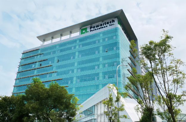
Taiwan’s Powertech Technology is moving to bring panel-level packaging into AI chip production. According to Nikkei, the company plans to begin production at what it says will be the world’s first panel-level chip packaging facility for AI chips as early as 2027, targeting server CPUs, AI computing chips, and advanced optics. If the timeline holds, Powertech would move ahead of TSMC in adopting the next generation of packaging technology for AI chips.
Taipei Times notes that the company plans to invest NT$70 billion (US$2.2 billion) in its FOPLP facility, with installed capacity set to increase from 1,000 panels per month this year to 5,000 in 2028. Powertech is also building an FOPLP production line in Singapore through a joint venture with Broadcom, with Nikkei noting that the facility is scheduled to begin production around 2028.
Demand is already running ahead of the planned expansion. Taipei Times reports that Powertech’s FOPLP capacity has been fully booked by two major customers, with Chairman D.K. Tsai saying demand is secured through 2030. Economic Daily News adds that available capacity for 2027 has already been booked by customers including AMD and Broadcom, leaving no room for additional customers and highlighting strong demand from major AI chipmakers.
Inside Powertech’s PiFO Packaging Technology
At the center of the push is Powertech’s self-developed PiFO panel-level packaging technology. Economic Daily News notes that PiFO is expected to enter mass production around mid-2027 for AI chips integrating ASICs and high-bandwidth memory (HBM), reaching economies of scale. Optical engines (OE) could begin small-volume shipments by the end of 2026, while co-packaged optics (CPO) integrating optical components with ASICs are targeted for mass production in 2027.
Powertech states that PiFO forms a bottom redistribution layer (RDL) directly on a panel, using silicon bridge dies and micro-bump bonding to connect ASICs and HBM. An upper RDL is then formed on the molded surface before substrate bonding completes the AI packaging module.
The approach is conceptually similar to TSMC’s CoWoS-L and Intel’s EMIB, but differs in both manufacturing and substrate design, using square panels rather than the round wafers used in CoWoS. According to Economic Daily News, PiFO uses 510 × 515 mm square panels, with each panel producing around 45 to 90 units depending on package size, offering higher area utilization and better cost efficiency. Compared with EMIB, which requires cavities in the substrate to embed bridge dies, PiFO completes the silicon-bridge connection during packaging before using a conventional ABF substrate, offering greater process flexibility and potential yield advantages.
The advanced packaging expansion also marks a significant shift for a company historically focused on memory. Powertech has historically been best known as the world’s largest contract memory chip packaging and testing provider, with Micron, Kioxia, and SanDisk among its key customers. According to Nikkei, the company began R&D on advanced panel-level packaging as early as 2016.
Read more
- [News] TSMC’s 5.5-Reticle CoWoS Reportedly Tops 99% Yield; Flags Memory, ABF as AI Bottlenecks
- [News] Intel EMIB-T Push Gains Momentum as TSMC CoWoS Crunch Drives Spillover; Unimicron, ASE Stand to Benefit
(Photo credit: Powertech)


