[News] Nikon Develops Photo Assist Patterning to Simplify Glass Substrate Plating, Sample Work Available on Request
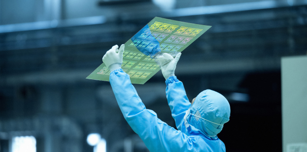
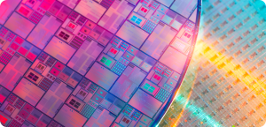
As demand grows for glass substrates driven by their superior heat resistance and lower warpage in advanced semiconductor packaging, equipment and materials suppliers are accelerating development efforts. Against this backdrop, Japan’s Nikon showcased its light-responsive surface treatment agent “PAP (Photo Assist Patterning)” at JPCA Show 2026, EE Times Japan reports, highlighting a simplified process that enables both surface smoothness and strong adhesion.
EE Times Japan, citing Nikon management, says the company expects glass substrate technology to be established around 2028 to 2030, and aims to position PAP as one of the available options for customers at that stage. According to the report, PAP is still under development, with Nikon already providing sample work upon request.
Two Key Bottlenecks Addressed in Glass Substrate Processing
As highlighted by the report, glass—being an insulating material—cannot undergo conventional electroplating, and its highly smooth surface makes it difficult for metals to adhere firmly.
To address this, two main approaches have been used, EE Times Japan notes: forming a thin film via vacuum sputtering before electroplating, or intentionally roughening the glass surface through etching to improve adhesion. However, the former requires expensive equipment, while the latter can degrade high-frequency performance due to increased surface roughness, the report explains, adding that Nikon’s newly developed PAP offers a simpler approach that addresses both key challenges by balancing surface smoothness and adhesion.
According to EE Times Japan, the material is coated across the entire substrate, and selective plating is achieved by applying light to targeted areas, which activates those regions to better retain the plating catalyst and enable metal deposition. Notably, Nikon’s development draws on its expertise in organic materials accumulated through its work in microscopes and cameras, the report says.
Meanwhile, a Nikon representative involved in PAP development, cited by the report, also highlighted that the film thickness is extremely thin, at under 10nm, meaning it does not compromise the substrate’s surface flatness.
The technology was also selected for the 22nd JPCA Awards, with JPCA noting its simplified electroless plating process for difficult-to-process glass and organic substrates, and its potential for improved manufacturability and reduced substrate damage compared with conventional methods.
Read more
(Photo credit: Nikon)