[News] Samsung Pushes Advanced Nodes, Reportedly Targets 1nm by 2030; 2nm Yields Top 60%
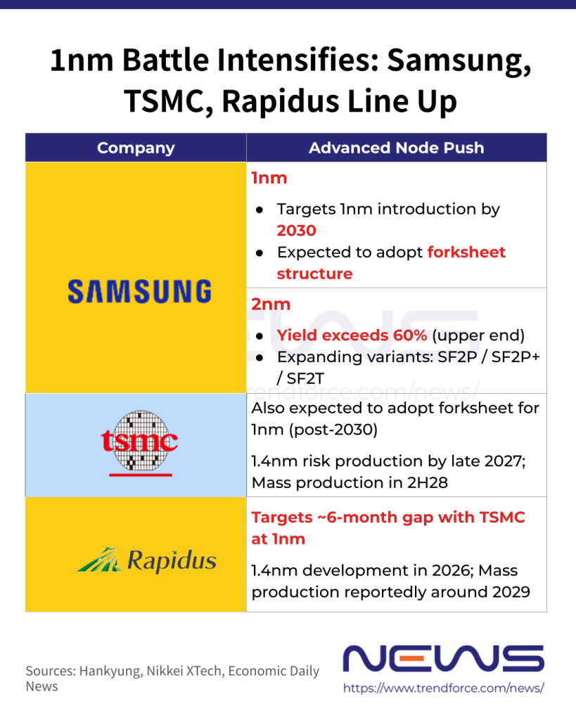
Samsung is intensifying its push into advanced semiconductor technologies. According to Hankyung, sources indicate that Samsung’s foundry division is targeting the introduction of a 1nm process by 2030. In parallel, the company plans to expand its lineup of process variants at the current leading-edge 2nm node to help secure major customers.
At the 1nm node, Samsung is expected to adopt new architectural innovations. As the report indicates, the process will incorporate a structure known as a forksheet. Up to the 2nm generation, Samsung has relied on gate-all-around (GAA) technology, which enhances power efficiency by enabling current to flow along all four sides of the channel rather than three.
Forksheet technology further tightens the spacing between GAA transistors by introducing insulating walls between them, akin to replacing open gaps between houses with solid barriers. By removing unused space, the same chip area can accommodate a greater number of transistors, the report adds.
Notably, the report indicates that TSMC is also expected to adopt forksheet structures for its own 1nm process beyond 2030. With its 1nm roadmap now outlined, Samsung is seen as positioning itself to compete with TSMC on more comparable technological footing.
Alongside its push toward 1nm, Samsung is also accelerating efforts to diversify its offerings at the current leading-edge 2nm node. Sources cited by the report note that, with 2nm yields now exceeding 60% at the upper end, productivity has improved markedly, strengthening expectations that the foundry business could return to profitability this year.
For Tesla’s 2nm AI chip “AI6,” Samsung is developing a tailored process known as SF2T. As the report notes, mass production is slated to begin in 2027 at the company’s new foundry facility in Taylor, Texas. Samsung is also accelerating the development of additional 2nm variants, including SF2P, which is set to be deployed from 2026 for next-generation smartphone application processors (APs) from its System LSI division, as well as SF2P+, which is expected to come online in 2027, the report adds.
Global Foundries Accelerate 1nm Push, Intensifying Competition
Meanwhile, beyond Samsung, major foundries are also pushing ahead with their 1nm roadmaps. According to Nikkei XTech, Rapidus CTO Kazunari Ishimaru said the company aims to narrow its technology gap with TSMC to around six months at the 1nm node. Nikkei XTech also notes that Rapidus plans to begin developing 1.4nm semiconductor manufacturing technology in 2026, with mass production reportedly targeted for around 2029.
By comparison, Economic Daily News reports that TSMC’s 1.4nm process could be rolled out earlier at its Central Taiwan Science Park site, with the first fab expected to complete trial production by late 2027 and move into mass production in the second half of 2028.
Read more
- [News] Rapidus Accelerates 1nm Push, Reportedly Targets Six-Month Gap with TSMC
- [News] Samsung Foundry Reportedly Expects 30%+ 2nm Order Growth in 2026; 1.4nm Set for 2029
(Photo credit: Samsung)