[News] South Korea Reportedly Tackles 3D NAND Bottleneck with New Material, Achieving Up to 23× Faster Erase Speed
South Korean researchers have developed tech using new material that may overcome the limitations of NAND flash memory. According to E-Patent News, a research team led by Professor Cho Byung-jin from the School of Electrical Engineering at the Korea Advanced Institute of Science and Technology (KAIST) has developed a new technology that addresses these limitations. By implementing a “smart gate” concept within semiconductors, the breakthrough enables simultaneous improvements in data processing speed and storage stability.
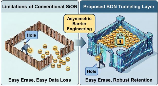
In particular, the research team developed an asymmetric tunneling layer technology that selectively controls electron movement using the new material boron oxynitride (BON). As the report points out, the approach is gaining attention for fundamentally addressing performance degradation and reliability issues associated with the scaling and stacking of 3D V-NAND structures.
As the report notes, NAND flash is a non-volatile memory that retains data even when power is turned off. However, as cells continue to shrink and stacking structures grow more complex, inherent limitations arise, including slower erase speeds and increased data leakage. These challenges become even more pronounced in next-generation penta-level cell (PLC) technology, which stores five bits per cell, making it one of the most difficult technical hurdles to achieve both high capacity and reliability simultaneously.
The research team tackled this issue by incorporating BON into the tunneling layer in place of conventional silicon-based materials. According to the report, BON creates different energy barriers depending on the type of charge, enabling holes—required during data erasure—to pass through more easily while preventing electrons, which represent stored data, from leaking out.
Performance Breakthrough: 23× Speed Gain and Higher Precision
Notably, as the report indicates, experimental results showed that BON-based devices delivered up to a 23-fold improvement in data erase speed compared to conventional designs, while maintaining high durability with minimal performance degradation during repeated operations.
Building on this, according to Chosun Biz, the researchers successfully differentiated 32 finely segmented voltage states in a penta-level cell (PLC) environment. This enabled them to control data distribution across devices with more than three times greater precision than before. As DigitalToday notes, the approach minimizes data interference, significantly lowering read error rates, and is regarded as overcoming the most critical technical hurdle facing penta-level cell NAND flash.
In addition, as E-Patent News adds, the technology is considered to have moved beyond the laboratory stage and is applicable to real semiconductor mass production processes, offering a practical breakthrough that could accelerate the commercialization of next-generation ultra-high-capacity memory.
Read more
- [News] While DDR5 Margins Reportedly Surpass HBM: What’s Next for Memory Giants?
- [News] Samsung and NVIDIA Team Up on Ferroelectric NAND R&D, Key Step Toward 1000-Layer NAND
(Photo credit: KAIST)