Popular Keywords
About TrendForce News
TrendForce News operates independently from our research team, curating key semiconductor and tech updates to support timely, informed decisions.
[News] Intel Ramps Up Advanced Packaging: Malaysia Complex Operational in 2026, EMIB Update
As industry buzz grows over Intel’s potential role in advanced packaging for NVIDIA’s next-gen Feynman GPUs at GTC 2026, eyes are on its EMIB (Embedded Multi-die Interconnect Bridge) technology and expanding Malaysia operations. According to The Edge Malaysia, the chipmaker’s advanced packaging complex and assembly operations are slated to become operational later this year.
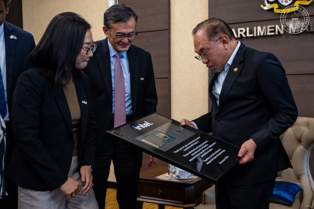
In a social media post cited by the report, Malaysian Prime Minister Datuk Seri Anwar Ibrahim revealed he had received a briefing from Intel CEO Tan Lip-Bu and his team on the latest progress of the company’s expansion plans in the country. Intel Foundry EVP and GM Naga Chandrasekaran, according to the report, outlined plans to kick off the first phase with assembly and testing capabilities for advanced packaging.
TechPowerUp previously reported that in late 2025, Intel has officially entered the final stage of its Project Pelican advanced packaging complex in Malaysia, with an additional $200 million investment to complete the site—already 99% finished. Notably, the site will handle die sort and prep operations and support both EMIB and Foveros packaging flows, enabling faster responses to customer needs, the report added.
Intel is also ramping up EMIB production through its long-time OSAT partner, Amkor. An earlier ETNews report suggested Intel has implemented its advanced packaging technology, EMIB, at Amkor’s Songdo K5 facility.
According to ETNews, EMIB (Embedded Multi-die Interconnect Bridge) is a 2.5D packaging technology connecting multiple semiconductor dies. Unlike traditional silicon interposers used in NVIDIA AI accelerators—which are costly—EMIB embeds silicon bridges directly into the chip substrate, providing a cheaper, more efficient way to achieve precise 2.5D packaging, the report noted.
Intel Advances EMIB Packaging
According to a recent ETNews report, Intel’s EMIB packaging is aiming for a sizable leap, targeting 120×120 mm packages—up from the industry-standard 100×100 mm used in NVIDIA’s latest AI chips, including Blackwell—marking a significant push in advanced semiconductor design.
ETNews adds that Intel plans to equip its 120×120 mm packages with at least 12 HBM stacks—up from the typical eight used in 100×100 mm designs. The company is also looking further ahead, targeting the introduction of even larger 120×180 mm packages by 2028, with enough capacity to accommodate up to 24 HBM stacks, the report suggests.
Notably, ETNews reports that after unveiling EMIB-T last year—an enhanced EMIB design incorporating through-silicon via (TSV) technology—Intel is now gearing this structure to support next-generation HBM4, which memory makers are ramping up for mass production.
However, the report highlights that challenges persist for Intel: while larger package sizes allow for more GPUs, CPUs, and memory like HBM to be integrated, they also increase manufacturing challenges, raising the risk of warpage and yield losses.
Read more
- [News] Intel to Inject $208M in Malaysia to Expand Chip Packaging Amid Soaring Demand
- [News] Intel Reportedly Taps Amkor’s Songdo Facility for EMIB Packaging in First-Ever Outsourcing Move
(Photo credit: Malaysian Prime Minister Datuk Seri Anwar Ibrahim’s X)
Please note that this article cites information from The Edge Malaysia, TechPowerUp, and ETNews.