Popular Keywords
About TrendForce News
TrendForce News operates independently from our research team, curating key semiconductor and tech updates to support timely, informed decisions.
[News] MediaTek CEO Flags Memory as One of XPU Bottlenecks, Now Making Up 50% of Costs
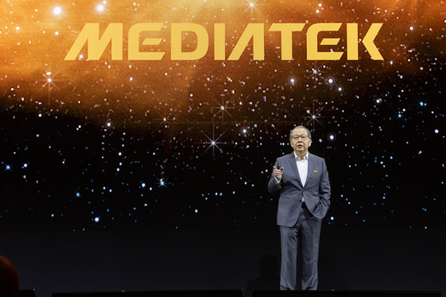
Joining Google’s TPU v8 program and emerging as a credible ASIC rival to global heavyweights like Broadcom, MediaTek is steadily strengthening its role in the AI ecosystem. Speaking at ISSCC in mid-February, CEO Rick Tsai outlined the four growing challenges facing XPU development, spanning compute, memory, interconnects, and advanced packaging technologies.
Memory Emerges as the Key Constraint in XPU Design
Among them, memory is increasingly becoming the defining constraint. Tsai noted that memory now accounts for roughly 50% of an XPU’s bill of materials, highlighting its growing influence on both system cost and overall performance.
Tsai explained that while AI training workloads continue to rely primarily on high-bandwidth memory (HBM), with solutions gradually shifting toward customized designs, inference is emerging as the next major growth engine. Under this shift, DDR DRAM is expected to see broader adoption due to its higher density and cost efficiency, with SRAM serving more selective use cases, he added.
Building on this shift, Tsai noted that the industry is accelerating exploration of new architectures — including compute-in-memory and near-memory computing — aimed at delivering lower power consumption alongside higher throughput.
Against this backdrop, both SK hynix and Samsung are advancing related developments. SK hynix, while pushing customized HBM that offloads select compute functions from GPUs and ASICs to the HBM base die, is also expanding its AI-focused DRAM roadmap under the AI-D lineup. The portfolio, as per the company, targets AI-era workloads beyond conventional DRAM, with solutions such as AI-D B (Breakthrough) emphasizing ultra-high capacity and flexible architectures designed to ease the memory wall, including CXL Memory Modules (CMM) and Processing-in-Memory (PIM).
Samsung, meanwhile, is among the earliest memory vendors commercializing PIM architectures for AI workloads. Back in 2021, Samsung announced the industry’s first HBM featuring built-in AI processing capabilities, dubbed HBM-PIM.
(Photo credit: MediaTek, ISSCC)
XPUs’ Packaging Push
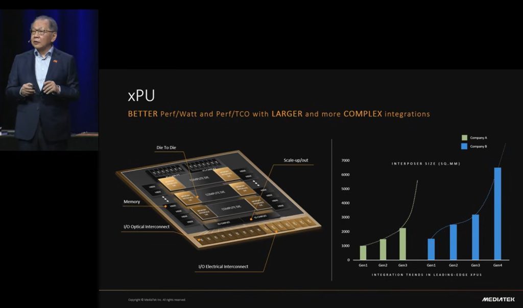
Additionally, Tsai highlighted the packaging challenges, emphasizing the need for improved power delivery and thermal management to handle the extreme energy demands of XPUs, ensuring they can deliver maximum compute performance. He noted that CoWoS (Chip on Wafer on Substrate) currently handles most 2.5D packaging and is expected to remain the leading solution for advanced packaging.
Interestingly, Tsai also pointed out that as the package size grows bigger, the technologies would become more complex as well. Tsai projected that by 2030, XPU package sizes could reach roughly 10,000 mm². He added that over time, package sizes could grow to 10,000–20,000 mm², comparable to an iPad Pro Max. Combined with 3D stacking of compute dies, this design is expected to dramatically improve performance per cost and performance per watt, he added.
Read more
- [News] Google Led TPU Innovation with Patent Spike; Broadcom, MediaTek Reportedly Boost Reserved Wafers
- [News] MediaTek Reportedly Secures Google v7e, v8e TPU Orders, Requests 7-Fold CoWoS Increase from TSMC
(Photo credit: MediaTek)