[News] TSMC 2nm Reportedly Tight Amid Mobile, HPC Demand; NVIDIA May Be First to Adopt 1.6nm in 2028
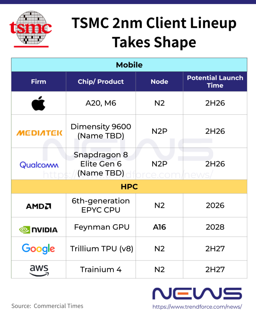
NVIDIA CEO Jensen Huang hosted a dinner on the evening of the 31st for senior executives from key supply-chain partners. As noted by Economic Daily News, Huang said TSMC must work at full stretch this year, underscoring tight capacity for its advanced nodes. TSMC’s 2nm capacity has reportedly been fully booked by orders from global tech giants. According to Commercial Times, industry sources say major players are accelerating plans to adopt TSMC’s 2nm process. AMD is said to target 2nm-based CPU production beginning in 2026, while Google and AWS are reportedly aiming for adoption in 3Q27 and 4Q27, respectively. NVIDIA, meanwhile, is said to plan the launch of its “Feynman AI” GPU in 2028, which is expected to adopt TSMC’s A16 process featuring backside power delivery, the report adds.
TSMC 2nm Capacity Tightens as AI and Mobile Demand Converge
Meanwhile, Commercial Times notes that both TSMC’s 2nm and 3nm are facing capacity constraints, as HPC and mobile chips compete for limited supply, with this year’s 2nm customers mainly Apple and Qualcomm. More specifically, Wccftech, citing sources, reports that Apple has secured more than half of the initial 2nm capacity.
Commercial Times adds that from 2027, general-purpose GPUs and ASICs are set to ramp more broadly, including AMD’s MI-series GPUs, Google’s eighth-generation TPU, and AWS’s Trainium 4. As the report notes, industry sources expect TSMC’s 2nm family to become a node with a long lifecycle, with its initial ramp likely to exceed that of the 3nm generation. N2 is set to enter mass production in 2026, followed by the N2P and A16 in the second half of the year, with A16 targeting select HPC products requiring complex routing and high-density power delivery.
Advanced Packaging Capacity Tightens Alongside 2nm
In addition, TSMC is upgrading its advanced packaging ecosystem. As Commercial Times indicates, as AI chips fully enter the era of chiplet architectures and ultra-large package sizes, single-die designs can no longer meet computing demands, making CoWoS-L, SoIC, and hybrid bonding effectively standard configurations.
Institutional investors cited by Commercial Times say TSMC is targeting more than 70% year-on-year growth in monthly CoWoS capacity by 2026, while gradually validating next-generation technologies such as CoWoP (Chip-on-Wafer-on-PCB) and CPO (co-packaged optics). However, the report adds that supply–demand imbalance remains the key bottleneck, as beyond tight 2nm foundry capacity, achieving high yields in large-scale system-level packaging is another major challenge.
Read more
- [News] TSMC Reportedly Suspends New 3nm Kick-offs, Steers Customers to 2nm to Optimize Costs
- [News] TSMC Reportedly Plans 2-nm Boost in Taiwan with Three New Fabs, NT$900B Investment
(Photo credit: TSMC)
Please note that this article cites information from Economic Daily News, Commercial Times, and Wccftech.


