Popular Keywords
About TrendForce News
TrendForce News operates independently from our research team, curating key semiconductor and tech updates to support timely, informed decisions.
[News] Japan Develops 10nm Nanoimprint Technology, with Potential to Tackle EUV Bottleneck
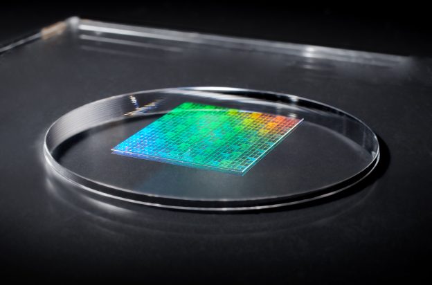
Japan’s Dai Nippon Printing (DNP) recently announced the successful development of nanoimprint lithography (NIL) technology with circuit line width as fine as 10 nanometers. The technology is designed for patterning 1.4nm-class logic semiconductor circuits. Customer evaluation has already begun, with mass production targeted for 2027. The company expects the technology to support continued miniaturization of advanced logic chips used in smartphones, data centers, NAND Flash, and other applications.
DNP plans to showcase the 10nm-linewidth NIL technology at SEMICON Japan 2025, to be held soon at Tokyo Big Sight.
As end-device performance continues to improve, demand for more advanced logic semiconductor nodes is steadily rising, driving the technical improvement of extreme ultraviolet (EUV) lithography. However, EUV requires massive capital investment for fab construction and lithography processes, while also posing challenges related to high energy consumption and environmental burden.
Against this backdrop, DNP has been continuously developing nanoimprint technology since 2003. By directly imprinting circuit patterns onto substrate materials, the approach offers chipmakers an alternative pathway to reduce lithography-related energy consumption and optimize cost structures in certain process steps.
Notably, the newly introduced 10nm-linewidth NIL technology can partially replace EUV lithography in selected patterning stages, providing semiconductor manufacturers that have yet to deploy EUV tools with another option for advanced logic processes. Moreover, ultra-fine semiconductor manufacturing based on nanoimprint technology can reduce energy consumption in the lithography process to approximately one-tenth of that of current mainstream processes.
Currently, DNP has been in discussion with semiconductor manufacturers and initiated evaluation programs for the new NIL technology. The company said it will continue to advance nanoimprint technology and expand production capacity in line with future market ramp-ups, positioning the business as a key growth driver within its semiconductor segment.
(Photo credit: Dai Nippon Printing)
Please note that this article cites information from Dai Nippon Printing (DNP).