Popular Keywords
- About Us
-
Research Report
Research Directory
Semiconductors
LED
Consumer Electronics
Emerging Technologies
- Selected Topics
- Membership
- Price Trends
- Press Center
- News
- Events
- Contact Us
- AI Agent
About TrendForce News
TrendForce News operates independently from our research team, curating key semiconductor and tech updates to support timely, informed decisions.
- Home
- News
[News] Intel Fab 52 Reportedly Rivals TSMC Arizona Phase 1 and 2 Combined Capacity on More Advanced 18A

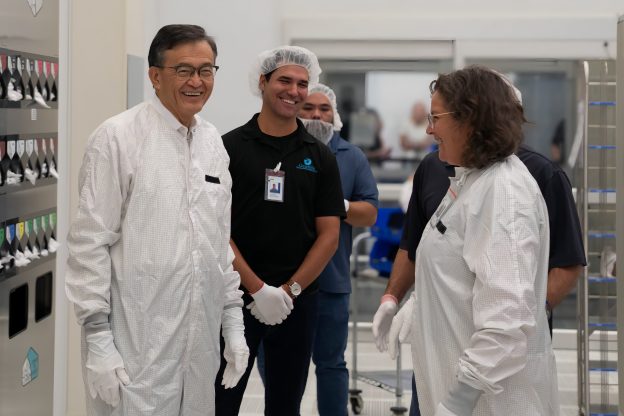
From a purely U.S. manufacturing perspective, Intel’s position remains firmly unshaken, with its Arizona Fab 52 said to exceed TSMC’s Fab 21 in both capacity and process technology. According to Tom’s Hardware, Fab 52’s capacity is comparable to the combined output of TSMC’s Fab 21 Phase 1 and Phase 2. The report further notes that, relative to Fab 21 Phase 1—which manufactures chips using TSMC’s N4 and N5—Intel’s Fab 52 can handle roughly twice the number of wafers per month while producing chips on its more advanced 18A process.
Team Blue’s Fab 52 is designed to manufacture chips using its 18A (1.8nm-class) process and more advanced nodes, incorporating gate-all-around (GAA) RibbonFET transistors along with the PowerVia backside power delivery network, as the report notes. Citing CNBC, it also indicates that the facility’s production capacity stands at around 10,000 wafer starts per week, equivalent to approximately 40,000 wafer starts per month (WSPM) once fully ramped.
Notably, the report adds that TSMC typically constructs fab modules with a production capacity of about 20,000 WSPM. As a result, even after TSMC completes its N3-capable Fab 21 Phase 2, Intel’s Fab 52 is expected to remain broadly on par with, or slightly ahead of, TSMC’s Arizona facilities once all three fabs reach full ramp-up.
For now, however, Intel’s facility has yet to reach full utilization, the report notes. Intel expects yields on its 18A process to reach world-class levels in early 2027, and until then, CPU production on this node will remain capped, leaving part of the fab’s capacity unused. In addition to Fab 52, Intel’s Fab 62 in Arizona is expected to be ready around 2028, CNBC adds.
Meanwhile, TSMC is reportedly moving to accelerate advanced chip production in the U.S. According to Nikkei, sources say the company plans to begin installing chipmaking equipment at its Arizona phase 2 around the summer of 2026, laying the groundwork for 3nm manufacturing in 2027.
Intel Boosts Fab 52 With ASML EUV Tools
Beyond its large capacity, Intel’s Fab 52 is also said to house a substantial amount of chipmaking equipment from ASML. According to Tom’s Hardware, citing sources, the facility is currently equipped with four ASML Twinscan NXE Low-NA EUV lithography systems, including at least one NXE:3800E, ASML’s most advanced Low-NA EUV tool. The NXE:3800E incorporates key components—such as the wafer handler, faster wafer stages, and light source—derived from next-generation High-NA EUV systems, enabling throughput of up to 220 wafers per hour at a 30 mJ/cm² exposure dose.
As CNBC reports, Intel has said that Fab 52 will ultimately house at least 15 EUV lithography systems. However, Tom’s Hardware notes that it remains unclear how many of these tools will be High-NA EUV systems.
Read more
- [News] Intel Gains Momentum: 18A Eyes Apple, EMIB Reportedly Tapped for Google-MediaTek TPUs
- [News] Intel Completes First 2nd-Gen High-NA EUV Acceptance Testing; ASML Eyes 2027–28 Mass Production
(Photo credit: Intel)


