Popular Keywords
About TrendForce News
TrendForce News operates independently from our research team, curating key semiconductor and tech updates to support timely, informed decisions.
[News] NVIDIA May Be TSMC’s Only A16 Customer So Far While Apple Reportedly Yet to Start Talks
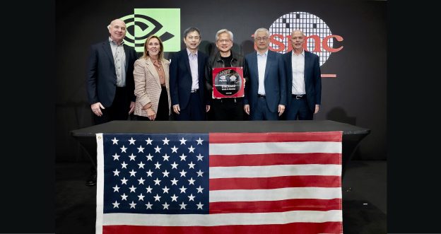
NVIDIA recently marked a major milestone, celebrating the first Blackwell wafer produced on U.S. soil at TSMC’s fab—an achievement that underscores their deepening partnership. That collaboration may soon expand further. According to South Korean outlet EBN News, citing industry sources, NVIDIA is currently the sole customer for TSMC’s forthcoming “A16” node, with the two companies conducting joint testing ahead of its expected deployment around 2027. This would mark a key turning point, as it would be the first time AI applications lead the adoption of TSMC’s most advanced process technology, as noted by Commercial Times.
Meanwhile, EBN News, citing sources, adds that Apple has yet to begin discussions with TSMC about adopting the A16 process for its mobile application processors (APs).
NVIDIA’s GPU roadmap progresses from Hopper to Blackwell, Rubin, and finally Feynman. The Blackwell lineup is currently in production, while Rubin is scheduled for launch next year. As EBN News notes, the Feynman GPU, planned for 2028, is expected to be built using TSMC’s A16 process. Although its release is still about three years away, the company is likely to begin ramping up A16 production in the second half of 2027, allowing roughly a year to optimize yield and manufacturing efficiency.
Rising Costs Loom as NVIDIA Prepares to Adopt TSMC’s A16 Node
The report from EBN News notes that NVIDIA has so far refrained from using TSMC’s most advanced nodes for its GPUs. Hopper and Blackwell are built on the 4nm process, while Rubin uses 3nm technology. This strategy, the report adds, has allowed the company to maintain exceptionally high operating profit margins—reaching 61% in the second quarter of fiscal 2026.
However, EBN News highlights that cost pressures are expected to mount starting with the Feynman generation, as NVIDIA transitions to TSMC’s most advanced node. With the foundry sharply raising prices for its most advanced processes, manufacturing costs are projected to rise significantly between 2027 and 2028, the report adds.
TSMC’s website notes that A16 integrates advanced nanosheet transistors with its Super Power Rail (SPR) solution. Compared with the N2P process, A16 delivers an 8–10% speed gain at the same voltage, a 15–20% power reduction at the same speed, and up to 1.1× chip density, making it well suited for high-performance computing (HPC) applications.
Read more
- [News] Apple Reportedly Takes Most of TSMC’s 2nm Capacity for A20 Series in Foldable iPhone and iPhone 18
- [News] NVIDIA May Be Among the First to Adopt TSMC A16 for 2028 Feynman Architecture
(Photo credit: NVIDIA)
Please note that this article cites information from EBN News, Commercial Times, and TSMC.