Popular Keywords
- About Us
-
Research Report
Research Directory
Semiconductors
LED
Consumer Electronics
Emerging Technologies
- Selected Topics
- Membership
- Price Trends
- Press Center
- News
- Events
- Contact Us
- AI Agent
About TrendForce News
TrendForce News operates independently from our research team, curating key semiconductor and tech updates to support timely, informed decisions.
- Home
- News
[News] SK hynix Second-Gen 3Gb DDR5 ‘A-Die’ Reportedly Spotted; Could Hit 7200 MT/s for Intel CPUs

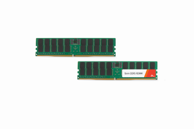
As memory giants race to advance their HBM roadmaps, DDR5 continues to be a key battleground in the push toward high-end memory. According to Wccftech, citing a leaker from Team Group, a new generation of SK hynix DDR5 has surfaced online. The chips appear to be second-generation 3Gb A-die memory implied by its X021 label, poised to replace the current 3Gb M-die that powers early DDR5 kits, the report suggests.
The report adds that, although SK hynix has yet to officially announce the new 3Gb DDR5 A-Die, the recently shared photo offers early hints about the chip. Following SK hynix’s naming convention—where letter pairs like EB, GB, and HB correspond to JEDEC speeds of 4800, 5600, and 6400 MT/s—the new “KB” designation in the part code “AKBD” likely points to 7200 MT/s, according to a post by a Team Group member, as noted by Wccftech.
Notably, Wccftech highlights that the timing aligns with Intel’s platform roadmap, as Panther Lake CPUs, expected in late 2025, and Arrow Lake Refresh, scheduled for 2026, are set to support DDR5-7200. This marks a significant leap from Raptor Lake’s DDR5-5600 and Arrow Lake’s DDR5-6400, suggesting that the new A-Die chips could form the backbone of next-generation high-speed memory kits for Intel’s upcoming processors, the report says.
For context, a previous Zhihu article pointed out that Samsung reigned supreme during the DDR4 era, with premium memory modules almost universally featuring Samsung’s specially-binned B-die chips. The DDR5 era, however, has seen SK hynix surge to the forefront, particularly with its A-die and M-die chips stealing the spotlight, the article noted.
However, the latest 3Gb DDR5 A-Die spotted appears to feature an 8-layer PCB, which could limit stability at higher memory speeds, Wccftech reports. While SK hynix seems to have produced early sample chips, sustaining speeds above 8000 MT/s on an 8-layer PCB remains challenging, the report notes, adding that to fully leverage the new A-Die “AKBD” chips, memory manufacturers will need to pair them with 10- or 12-layer PCBs.
Read more
(Photo credit: SK hynix)


