Popular Keywords
- About Us
-
Research Report
Research Directory
Semiconductors
LED
Consumer Electronics
Emerging Technologies
- Selected Topics
- Membership
- Price Trends
- Press Center
- News
- Events
- Contact Us
- AI Agent
About TrendForce News
TrendForce News operates independently from our research team, curating key semiconductor and tech updates to support timely, informed decisions.
- Home
- News
[News] What Comes After HBM? NAND-Stacked HBF May Power AI’s Future

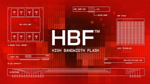
According to The Elec, KAIST Professor Kim Jeong-ho noted that HBF (High Bandwidth Flash)—NAND flash stacked like HBM—could become a decisive factor for the future of AI. As the report explains, HBF resembles HBM in structure, with dies stacked and linked by through-silicon vias (TSVs). The key distinction is that HBF uses NAND flash in place of DRAM.
AI Bottlenecks Highly Influenced by Memory Bandwidth
As the report notes, Kim highlighted that current AI is bottlenecked by memory bandwidth and capacity. He explained that today’s Transformer-based models may process sequences of up to 1 million tokens, requiring terabytes of data. When this data must be read and written thousands of times per second, limited bandwidth creates slowdowns for large language model (LLM) services like OpenAI’s ChatGPT or Google’s Gemini.
As cited by the report, Kim explained that the bottleneck arises from the von Neumann architecture—the fundamental design of modern computers—where the CPU or GPU is physically separated from memory, making data transfer bandwidth between them critical.
Beyond DRAM: How HBF Could Power Future AI
To address these challenges—particularly as future AI demand might expand to generating movie-length videos that would require memory capacities more than 1,000 times greater than today’s—Kim emphasized that slower but higher-capacity NAND flash could serve as a complement. He explained that while NAND flash is slower than DRAM, it provides about 10 times the capacity, which may be essential for supporting next-generation AI.
Kim emphasized that HBF could help overcome HBM’s limited capacity by directly storing large AI models on the GPU. In this framework, HBM functions as a cache for rapid data processing, while HBF stores the massive AI models themselves, he stated, as cited by the report.
Notably, U.S. NAND leader SanDisk disclosed earlier this year that it is developing HBF technology and has signed a landmark MoU with SK hynix to jointly define specifications, according to its press release. SanDisk plans to deliver HBF samples in 2H26, with the first AI inference devices expected by early 2027. Its first-generation HBF will reportedly feature 16-layer memory, offering up to 512GB per stack—matching HBM’s bandwidth while increasing capacity by 8 to 16 times.
Read more
- [News] Memory Giants SanDisk, SK hynix Unite for HBF Standard, with Samples Expected in 2H26
- [News] Kioxia Reportedly Eyes 2027 Launch for NVIDIA-Partnered AI SSDs with 100x Speed Boost
(Photo credit: SanDisk)


