Popular Keywords
About TrendForce News
TrendForce News operates independently from our research team, curating key semiconductor and tech updates to support timely, informed decisions.
[News] Resonac Teams up with Applied Materials, TEL and Other Chip Giants on Panel-level Interposers
As fan-out panel-level packaging (FOPLP) gains traction among semiconductor leaders like TSMC, Japanese companies—long known for their materials expertise—are stepping into the spotlight as well.
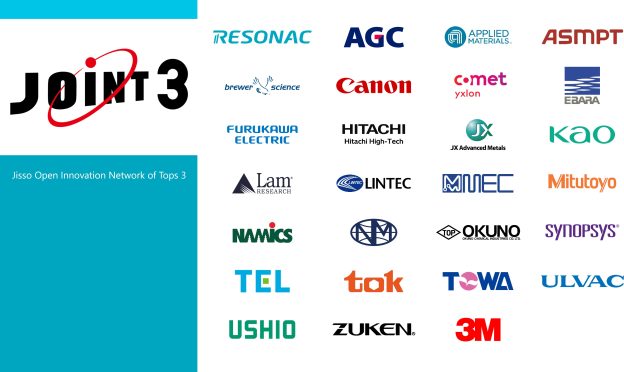
Resonac, according to Nikkei and its press release, has announced JOINT3, a joint development framework formed with 26 global tech players, including chipmaking tool titans Applied Materials, Tokyo Electron and Lam Research. Notably, the initiative will focus on creating materials, equipment, and design tools for panel-level organic interposers.
Development will be supported by a prototype production line capable of manufacturing 515 x 510mm organic panels, Resonac said, adding that the production line is expected to begin operations in 2026.
As per Nikkei, Resonac also announced plans to build a dedicated R&D center in Japan’s Ibaraki Prefecture, north of Tokyo, featuring the aforementioned prototype production line. The five-year project will cost ¥26 billion (approx. $174 million) and be jointly funded and operated by member companies, the company said.
FOPLP Moves from Semiconductor Giants
In addition to Resonac and its allies, other semiconductor giants also embrace FOPLP for larger, more efficient chip designs, Japan’s Nikon, according to its press release, has begun taking orders in July for its new DSP-100 digital lithography system, designed specifically for 600 mm square panels used in advanced AI chip packaging.
Traditional foundries and chip packaging leaders are among the most aggressive adopters of the technology. According to Economic Daily News, key players such as TSMC, ASE, and Powertech are ramping up investments to meet growing demand for high-performance computing (HPC) chip packaging from major clients like NVIDIA and AMD.
Another Economic Daily News report notes that TSMC is currently building a pilot production line in Taoyuan, Taiwan, with limited trial production anticipated to begin as early as 2027. However, TSMC’s first-generation FOPLP (CoPoS, Chip-on-Panel-on-Substrate), is expected to use a 300mm x 300mm panel—smaller than the previously tested 510mm x 515mm format, the report adds.
Economic Daily News also suggests TSMC is reportedly set to introduce its latest FOPLP technology in the U.S. to meet rising demand from customers seeking chips manufactured in the U.S.
Read more
- [News] TSMC Reportedly to Bring FOPLP Packaging Tech to U.S., Trial Production May Start in 2027
- [News] TSMC Rumored to Begin FOPLP Production with Smaller Substrates, with Mini Lines Prepared by 2026
(Photo credit: Resonac)
Please note that this article cites information from Nikkei, Economic Daily News, Resonac, and Nikon.