Popular Keywords
- About Us
-
Research Report
Research Directory
Semiconductors
LED
Consumer Electronics
Emerging Technologies
- Selected Topics
- Membership
- Price Trends
- Press Center
- News
- Events
- Contact Us
- AI Agent
About TrendForce News
TrendForce News operates independently from our research team, curating key semiconductor and tech updates to support timely, informed decisions.
- Home
- News
[News] China’s AMEC Reportedly Saw Plasma Etching Grow at 50% CAGR, Backs 5nm Without EUV

As U.S. chip export controls tighten, China is fast-tracking its push for semiconductor self-sufficiency. Alongside Naura Technology and Huawei-linked SiCarrier, etching equipment leader AMEC is also rising rapidly. According to local media Science and Technology Innovation Express News, from 2019 to 2024, AMEC saw its plasma etching revenue grow at a CAGR of over 50%.
With market rumors that Huawei and SMIC have achieved 5nm chip production and aim for 3nm mass production next year, AMEC Chairman Gerald Yin confirmed that 5nm nodes can be reached using DUV lithography through more complex double or multi-patterning, as per Science and Technology Innovation Express News.
While the feasibility of 3nm remains uncertain without EUV tools, AMEC plans to push node scaling by combining advanced etching with multi-patterning techniques, according to the report.
Notably, back in 2018, AMEC’s 5nm plasma etching tools are reportedly verified by TSMC, according to Design & Reuse.
Another ijiwei report notes that AMEC announced several of its advanced logic etching tools have passed customer validation and are gaining market share in China’s advanced logic production lines. Notably, the report suggests that AMEC’s high aspect ratio etching and metal film deposition tools are shipping in volume to advanced domestic memory fabs.
Science and Technology Innovation Express News indicates that over the past two decades, AMEC has rolled out 18 models of etching tools in total.
AMEC’s Growing Ambitions
On the other hand, ijiwei reveals that in 2024, AMEC ramped up its R&D investment to RMB 2.45 billion—a 94.3% increase from the previous year—making up over 27% of its total revenue. The company is reportedly developing more than 20 new tools across six key categories, including thin film deposition systems like MOCVD (Metal-Organic Chemical Vapor Deposition), LPCVD (Low Pressure Chemical Vapor Deposition), EPI, and ALD (Atomic layer deposition).
According to Science and Technology Innovation Express News, AMEC plans to localize over 20 thin-film tools currently under export restrictions, with full development targeted by 2029.
The report, citing Yin, notes that AMEC’s tools cover about 30% of semiconductor equipment needs. Over the next 5 to 10 years, it aims to expand that to 60%—including etching, thin-film, metrology, and some wet process tools, the report adds.
Read more
- [News] SMIC Reported to Complete 5nm Chips by 2025, but Costs May Be 50% Higher Than TSMC’s
- [News] China’s SiCarrier Reportedly Eyes DUV Breakthroughs for 5nm, Debuting Products This Week
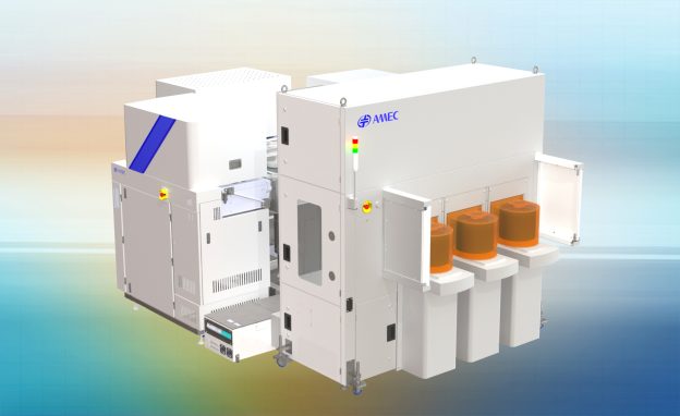
(Photo crredit: AMEC)


