





 Download Report
 Contact Us
The 3XX-Layer NAND Generation—An Inevitable Architectural Transition and the Rise of Base Dies

Last Modified
2026-04-27

Update Frequency
Aperiodically

Format
Driven by AI, next-generation advanced NAND has become the mainstream. As traditional vertical stacking encounters physical limitations and performance degradation, the industry's focus is shifting toward architectural innovation. By leveraging heterogeneous integration technology—which separates the manufacturing of logic circuits and memory before vertically bonding them—manufacturers can overcome transmission bottlenecks and secure a future competitive advantage.
Key Highlights
- AI Demand: Advanced NAND is now the industry's core focus for high-end storage.
- Physical Limits: Vertical stacking faces severe etching and signal delay hurdles.
- Architecture Shift: Logic and memory are built separately, then hybrid bonded.
- Future Focus: Success relies on heterogeneous integration and foundry partnerships.
Table of Contents
- 2XX-Layer Technology Takes Center Stage as AI Drives Technological Upgrades
- Comparison of 3XX-L Product Specifications Among the Top Six NAND Flash Suppliers
- The Performance Limits of CMOS Stacking: 300 Layers Represents a Major Hurdle
- Read/Write Performance Degradation Due to Increased Layer Counts (Illustration of RC Delay)
- Base Die/Peripheral Die and CBA Architecture: Reassignment of Labor between Logic and Memory
- Cross-Sectional Comparison of NAND Architectures: Conventional CUA v.s. CBA/Xtacking
- From Race of Stacking to Competition of Architectures: Industry Logic after 3XX-L
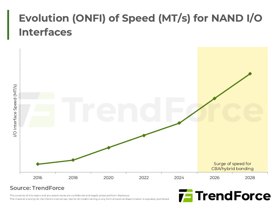
- Evolution (ONFI) of Speed (MT/s) for NAND I/O Interfaces
<Total Pages: 6>

Spotlight Report
-

DRAM Monthly Datasheet Oct. 2026
2026/10/16
Semiconductors
EXCEL
-

NAND Flash Monthly Datasheet Oct. 2026
2026/10/15
Semiconductors
EXCEL
-

Global Memory Supply-Demand Divergence: Analyzing 2027 DRAM Structural Tightness and NAND Flash Oversupply
2026/07/28
Semiconductors
PDF
-

4Q26 Memory Price Forecast
2026/09/24
Semiconductors
PDF
-

Memory Market Outlook: 2026-2027 DRAM & NAND Revenue and Capex Analysis
2026/10/01
Semiconductors
PDF
-

DRAM Contract Price Aug. 2026
2026/08/31
Semiconductors
PDF
NAND Flash PlatinumRelated Reports




Download Report
18,000

Membership
Spotlight Report
-
DRAM Monthly Datasheet Oct. 2026
2026/10/16
Semiconductors
EXCEL
-
NAND Flash Monthly Datasheet Oct. 2026
2026/10/15
Semiconductors
EXCEL
-
Global Memory Supply-Demand Divergence: Analyzing 2027 DRAM Structural Tightness and NAND Flash Oversupply
2026/07/28
Semiconductors
PDF
-
4Q26 Memory Price Forecast
2026/09/24
Semiconductors
PDF
-
Memory Market Outlook: 2026-2027 DRAM & NAND Revenue and Capex Analysis
2026/10/01
Semiconductors
PDF
-
DRAM Contract Price Aug. 2026
2026/08/31
Semiconductors
PDF