Popular Keywords


AMD
News
[News] CPU Prices Reportedly Diverge as Consumer Stays Flat Despite Potential 15% Server-Grade Hikes
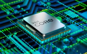
To what extent are CPU prices rising, and how is this playing out in the consumer market? Despite growing speculation about price hikes, a report by Cailian Press finds that consumer CPU prices have so far remained largely stable. According to the report, based on observations in Shenzhen’s Huaqia...
News
[News] Intel Recruits Qualcomm and AMD GPU Veteran Eric Demers to Advance AI Push
Intel has brought in a veteran GPU architect to strengthen its AI efforts. According to Tom’s Hardware, Eric Demers, who designed many of the leading GPUs at ATI Technologies, later acquired by AMD, and went on to lead Qualcomm’s GPU designs, has joined Intel with a focus on AI. Demers will serv...
News
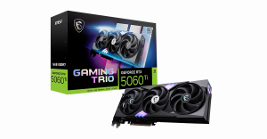
[News] VRAM Shortage Reportedly Drives NVIDIA’s RTX 50 Price Hikes at Taiwan’s GPU Card Makers This Month
While earlier reports from Wccftech said NVIDIA was reshuffling RTX 50 series supply toward 8GB GeForce RTX 5060 and 5060 Ti models amid memory shortages, the impact now appears to be spreading across Taiwan’s major graphics card makers. According to Commercial Times, MSI has already moved to rais...
News

[News] Trump Targets NVIDIA H200, AMD MI325X with 25% Tariff; U.S. Infrastructure Spared
The White House has issued a new order on semiconductor tariffs. According to Reuters, U.S. President Donald Trump on Wednesday imposed a 25% tariff on select AI chips, including NVIDIA's H200 AI processor and a comparable product from AMD, the MI325X. Chips imported to support building up the U....
News

[News] AMD Reportedly Weighs Reviving Older Zen 3 Chips as DDR5 Prices Push Up PC Upgrade Costs
As memory shortages continue to drive costs higher, chipmakers are reassessing their strategies. According to Tom’s Hardware, David McAfee, AMD’s Corporate Vice President and General Manager of the Client Channel Business, said at CES 2026 that the company could consider reviving older AM4 desk...
- Page 2
- 31 page(s)
- 152 result(s)