


[News] JSG Achieved Breakthrough in 12-inch SiC Crystal Growth
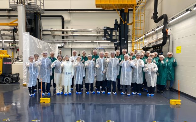
On August 24, JSG (Jingsheng Mechanical & Electrical) released an investor relations record detailing the latest progress across its semiconductor equipment, silicon carbide (SiC) substrate, and diamond materials segments.
SiC Substrate & Global Capacity Expansion
- Technical Breakthrough: Leveraging in-house developed SiC single-crystal growth furnaces and iterative 8- to 12-inch growth processes, JSG optimized thermal field designs and gas-phase precursor distribution. The company resolved core industry challenges—such as thermal field non-uniformity and crystal cracking—to achieve a key technical breakthrough in 12-inch ultra-large-size SiC crystal growth.
- Commercialization: Customer sampling and verification are underway. JSG has achieved mass production for 8-inch SiC substrates and small-batch supply for 12-inch substrates.
- Global Footprint: JSG is building an 8-inch SiC substrate industrialization facility in Penang, Malaysia, and an 8-inch SiC substrate-supporting crystal project in Yinchuan, China. This dual-base framework aims to accelerate the commissioning of a project targeting an annual capacity of 900,000 6-inch and 8-inch SiC substrates. The Penang site is slated for production in 2027.
Diamond Materials & Semiconductor Equipment
- Diamond Materials: JSG completed key technical research on large-size diamond wafer materials, successfully developing 8-inch polycrystalline diamond wafers. The company has mastered growth processes for 1- to 8-inch full-specification wafers and established a high-volume manufacturing (HVM) line for large-size diamond.
- Semiconductor Equipment: JSG commercialized its 12-inch epitaxy (Epi) equipment and entered top-tier fabs for verification of its Atomic Layer Deposition (ALD) systems.
(Photo credit: JSG)


