


[News] Micron Warns AI Memory Wall Worsens; Cites HBM in 17% of Meta Llama 3 Training Interruptions
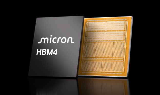
At Hot Chips 2026, Micron highlighted the growing “memory wall” challenge as AI compute advances outpace memory improvements. As noted by Maeil Business Newspaper, Micron Fellow Raghu Sriramaneni, who specializes in HBM design architecture, warned that the gap may be worsening in the AI era. He noted that AI accelerator compute performance roughly triples every two years, while High Bandwidth Memory (HBM) bandwidth grows by less than twofold over the same period.
The growing reliance on HBM also raises reliability challenges. Wccftech reports that Micron cited Meta’s Llama 3 data showing that HBM failures accounted for roughly 17% of unintended training interruptions. Sriramaneni also stressed that new designs that blur the boundary between compute and memory could offer one path to overcoming the bottleneck.
HBM scaling also brings a growing footprint and supply burden. Sriramaneni pointed to a latest-generation package integrating two GPUs with eight 12-layer HBM4 stacks, where memory accounts for roughly 90% of the semiconductor area, more than eight times the area occupied by the GPUs. Meanwhile, producing the same memory capacity with HBM requires roughly three times as many wafers as standard DDR5 DRAM, adding further pressure on production capacity.
Thermal management is also becoming a critical constraint. As noted by Cailian Press, Sriramaneni said rising data transfer speeds have made heat dissipation a primary design consideration. In HBM’s multilayer structure, the bottom layers generate the most heat, while cooling occurs from the top, requiring heat to travel through the entire stack. He added that liquid cooling and ultra-thin chip technologies are emerging as potential solutions, with chip structures increasingly being designed around thermal requirements from the outset.
Micron Explores Next-Gen Packaging to Tackle HBM Thermal Challenges
To address these growing constraints, Micron is looking beyond conventional HBM design to advances in interconnects, packaging, and cooling. ServeTheHome notes that Micron is exploring technologies to address HBM scaling challenges, including memory-optimized SerDes and die-to-die PHY (Physical Layer) for faster I/O, along with larger SiPs and glass substrates for advanced packaging. For thermal management, the company highlighted liquid cooling, hybrid bonding, and changes to solder and side-mold materials as potential solutions as higher DRAM activity, taller stacks, and more advanced base dies increase heat.
Wccftech adds that Micron is also developing fusion bonding, which supports single-digit-micron pitches and reduces dielectric layers between stacked DRAM dies, helping lower thermal resistance while enabling higher data throughput.
Read more
- [News] Micron’s Sanand Assembly & Test Plant Gets Boost With 12-Hour Shifts, First in Gujarat
- [News] Hot Chips 2026: Samsung’s zHBM Claims 70% Power-Efficiency Gain; SK hynix Evaluates Intel EMIB
(Photo credit: Micron)


