


[News] Korean and Japanese Researchers Unveil New AI Memory Architectures to Address HBM Thermal Limits
Research teams from South Korea and Japan have independently proposed two novel memory integration architectures aimed at increasing memory capacity and bandwidth without further increasing the height of high-bandwidth memory (HBM) stacks. Both approaches also seek to alleviate the growing thermal challenges facing AI accelerators.
The studies were presented at the 2026 IEEE/JSAP VLSI Technology and Circuits Symposium in June, sharing a common concept: positioning DRAM dies vertically on their edges rather than stacking them horizontally.
A team from the Ulsan National Institute of Science and Technology (UNIST) introduced a concept known as Vertical-Die (V-Die). The architecture arranges customized DRAM dies upright, eliminating through-silicon vias (TSVs) in favor of edge I/O connections at the bottom of each die while incorporating liquid-cooling channels between adjacent chips.
According to the researchers, the design delivers up to four times as many interconnects as HBM4 and reduces memory access latency by 37%. Simulations based on a 16-layer stack, H100-class hardware, and GPT-3-scale workloads showed V-Die achieving throughput of 540 tokens per second, significantly outperforming HBM4’s 296 tokens per second. Time-to-first-token (TTFT) was also reduced by 32% to approximately 24 milliseconds.
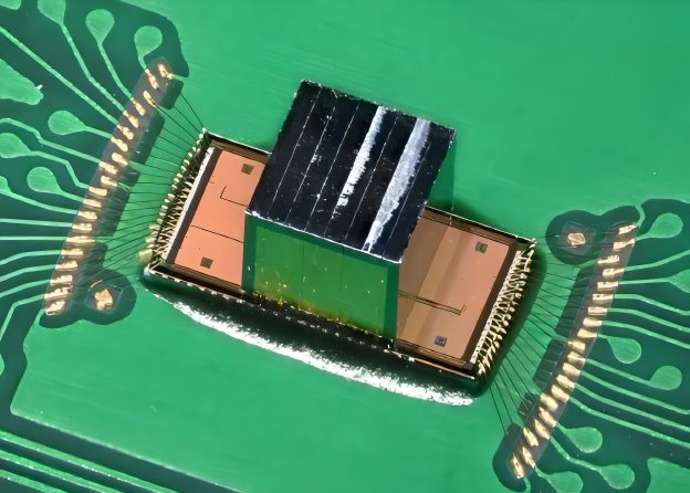
Meanwhile, researchers at the University of Tokyo focused on manufacturability with a design called MOSAIC. Since even slight variations in die thickness can cause alignment issues when chips are mounted on their edges, the team replaced conventional physical interconnects with contactless inductive coupling. Tiny coils enable data transmission across microscopic gaps, removing the need for every signal pad to align precisely with a physical contact.
The prototype interface supports data rates of up to 4 Gbps per channel. In a DRAM-on-GPU configuration, the architecture could double memory capacity compared with HBM4. Hardware demonstrations also indicate that the structure offers up to three times the thermal conductivity of conventional stacked memory while increasing memory capacity by as much as 30%.
Both projects target the increasingly severe “memory wall” confronting AI computing. Although modern AI accelerators provide enormous computational performance, large language models require continuous movement of massive datasets between processors and memory, making HBM a critical component of AI hardware. However, as memory stacks grow taller, heat dissipation becomes more difficult, while TSVs consume valuable die area and add complexity to signal integrity and advanced packaging.
Memory manufacturers including SK hynix, Samsung Electronics, and Micron are also working to improve thermal performance in next-generation products such as HBM4, iHBM, and HBM5. However, these developments continue to rely on the conventional vertically stacked architecture.
The researchers emphasized that neither V-Die nor MOSAIC is ready to replace commercial HBM. V-Die remains at the proposal stage, with prototype development underway to validate its electrical and thermal performance. MOSAIC has demonstrated proof-of-concept hardware but has yet to prove it can achieve the manufacturing yield, cost efficiency, and long-term reliability required for commercial DRAM production.
(Photo credit: The University of Tokyo)


