[News] China’s Yuanjiwei Eyes 5nm-Equivalent Chips Without EUV by 2029, Debuts 2D Semiconductor Pilot Line
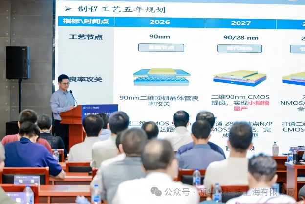
China has outlined another ambitious push in semiconductors. According to South China Morning Post, chip startup Yuanjiwei has launched what it describes as the world’s first pilot 8-inch production line for two-dimensional (2D) semiconductors. Looking ahead, the report adds that Chairman Bao Wenzhong said the company aims to establish a manufacturing process comparable to a 90nm silicon node by the end of 2026, before advancing to a fully domestic process equivalent to 5nm chips by 2029 without the use of extreme ultraviolet (EUV) lithography.
As part of this effort, IThome notes that Yuanjiwei has released version 0.1 of its 500nm process design kit (PDK) based on its 8-inch pilot line and launched foundry tape-out services. South China Morning Post says the developments mark China’s transition in 2D semiconductor technology from laboratory research to engineering validation and industrial production.
Why 2D Semiconductors Matter
Compared with conventional silicon-based chips, 2D semiconductors offer several potential advantages. According to South China Morning Post, the atomic-scale thickness of 2D materials enables further transistor scaling without relying on increasingly complex transistor architectures. The report adds that their ultra-low leakage characteristics could significantly reduce chip power consumption, while integration with technologies such as 3D stacking may also help increase memory chip capacity over time.
Meanwhile, as noted by STAR Market Daily, Yuanjiwei plans to advance heterogeneous integration by combining 2D and silicon-based chips, continuously enhancing its advanced packaging capabilities through technologies such as hybrid bonding, with the goal of building design and manufacturing platforms for 2.5D and quasi-3D ICs.
Potential Applications of 2D Semiconductors
On the application side, STAR Market Daily notes that the ultra-low leakage characteristics of 2D semiconductors could significantly reduce refresh power consumption, making them well suited for edge devices and high-performance computing applications. Combined with 3D stacking technology, they could also gradually increase DRAM capacity. The report adds that, as an ultra-thin silicon-on-insulator (SOI) material, 2D semiconductors also offer unique advantages for RF analog circuits, radiation-hardened communications, and brain-computer interfaces. The platform is also expected to support device development and manufacturing for emerging fields such as optoelectronic sensing and quantum computing.
Read more
- [News] Huawei Expands Tau Scaling Law V2 Paper, Highlighting LogicFolding Path to Ascend AI Chips in 2030
- [News] Chinese Team Achieved Major Breakthrough in Carbon Nanotube CFET Architecture
(Photo credit: Yuanjiwei)