[News] Chinese Equipment Maker Achieves Breakthrough in SiC Laser Lift-Off Technology
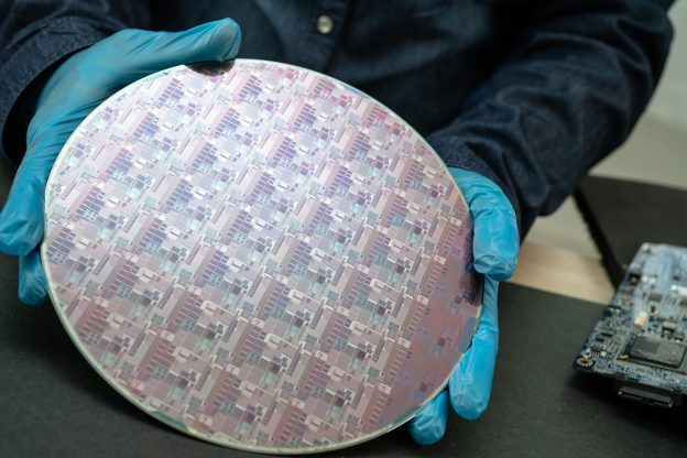
Chinese equipment supplier Zhongwei Precision Instrument has announced a major advance in silicon carbide (SiC) substrate manufacturing, becoming the first to achieve mass production of 8-inch SiC laser lift-off technology with total material loss reduced to the 40μm range.
The milestone breaks through the industry’s longstanding 60–80μm loss barrier and provides critical technological support for the large-scale industrialization of domestically produced large-diameter SiC wafers.
As SiC applications expand beyond electric vehicles and energy storage into high-tech sectors such as advanced packaging and RF communications, the 8-inch wafer format has emerged as the mainstream choice for capacity expansion due to its advantages in cost and productivity.
However, SiC remains one of the industry’s most challenging materials to process. With a hardness approaching that of diamond, the material is both brittle and difficult to machine. Traditional wire-saw cutting methods typically incur material losses of around 250μm and are prone to introducing microcracks, while also suffering from low throughput and high consumable costs.
Although laser lift-off technologies have gradually replaced conventional approaches, many existing systems continue to struggle with optical-path precision and energy uniformity limitations, preventing them from surpassing the 60μm material-loss threshold. Such constraints have made it difficult to satisfy the stringent requirements of automotive-grade and advanced packaging applications.
To address these challenges, Zhongwei Precision Instrument has focused on core laser-processing technologies, completing full-stack upgrades spanning equipment architecture, optical-path control and process algorithms. By leveraging self-developed laser sources, precision optical design and thermal-effect suppression algorithms, the company claims it can accurately control laser energy penetration depth and processing range while minimizing material damage.
As a result, the company has achieved stable total material loss of ≤40μm during mass production of 8-inch SiC substrates—more than 30% lower than mainstream industry levels and roughly 80% lower than conventional wire-cutting methods.
The technology enables a 400μm SiC ingot to consistently yield 350μm qualified substrate wafers. The process also adopts a greener production approach by eliminating consumables and chemical reagents, reducing secondary pollution risks while significantly improving wafer output per ingot.
Each wafer can be processed in under 15 minutes, improving throughput by 20–30 times compared with traditional methods. The system also supports continuous 24-hour mass production with stable yields and has already completed on-site validation and pilot-scale deployment at several leading SiC manufacturers.
(Photo credit: FREEPIK)