[News] Researchers Reportedly Develop Ultrafast Laser Wiring for Glass Substrates, Targeting CPO Bottleneck
As glass substrates gain traction as a key material for next-generation AI semiconductor packaging, related technologies are drawing increasing industry attention. According to ETNews, Chonnam National University said a research team led by Professor Han Seung-hoe from the Department of Mechanical Engineering has developed an “ultrashort-pulse laser-induced chemical vapor deposition (ULCVD)” technology.
The report indicates that the method uses an ultrafast femtosecond laser to directly inscribe conductive carbon circuits on both sides of transparent substrates without the need for masks, enabling flexible and selective wiring across the entire surface.
The breakthrough is expected to drive advances in devices based on three-dimensional (3D) glass structures, including optical–electrical convergence semiconductors built on advanced co-packaged optics (CPO), as well as high-precision quantum sensors, the report adds.
New Wiring Technology Tackles Glass Substrate Bottleneck in CPO
As the report indicates, glass substrates are becoming increasingly important for CPO, and the team’s proposed technology is expected to further support their adoption. It adds that next-generation CPO technology integrating electrical and optical light signals on a single chip has emerged, accelerating the use of glass substrates with superior optical properties.
However, forming three-dimensional interconnects in processes such as through-glass vias (TGV) and redistribution layers (RDL), which link the top and bottom surfaces of glass substrates, remains a significant technical challenge, the report notes.
The research team demonstrated that femtosecond lasers can pass through transparent glass, leveraging nonlinear absorption effects to enable flexible and selective wiring on both the front and back surfaces of glass substrates. The report adds that, through process optimization, the team achieved electrical conductivity comparable to the best laser-induced graphene (LIG) wiring reported in academia.
The technology was also confirmed to have strong potential to form interconnects inside through-holes and on complex 3D curved structures, which are critical for future semiconductor packaging, the report highlights.
Looking ahead, the report notes that Professor Han Seung-hoe said the team plans to expand the ULCVD process beyond current carbon-based wiring to include various metal materials such as copper (Cu) and gold (Au), which are expected to be key materials for future semiconductor packaging.
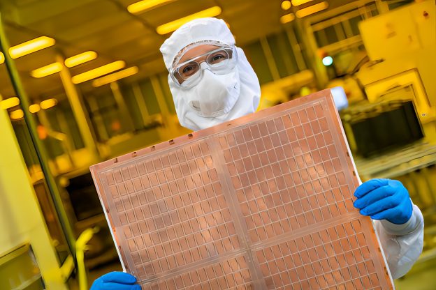
Commercialization of glass substrates is accelerating. According to Global Economic, citing sources, Intel has outlined a roadmap targeting 2030 to secure a technological edge. Meanwhile, South Korean firms are ramping up efforts. The report notes that, in response to Intel’s push, Absolics, a subsidiary of SKC, is building the world’s first mass-production facility for glass substrates in Georgia. While Intel remains at the research stage, Absolics aims to move into full-scale production first and secure an early lead in materials standards.
Read more
- [News] Korea Challenges Intel on Glass Substrate Standards as Absolics, Samsung Accelerate Commercialization
- [News] SKC Reportedly Channels Over Half of ₩1T Capital Increase Into Absolics to Fast-Track Glass Substrates
(Photo credit: Intel)