[News] Naura Reportedly Unveils Hybrid Bonding Tool at SEMICON China; SiCarrier, Last Year’s Lithography Standout, Misses Show
SEMICON China 2026, the largest semiconductor industry event in Shanghai, opened on March 25. According to STAR Market Daily, several Chinese chip equipment makers showcased their latest progress, with leading players including Naura, AMEC, Piotech, ACM Research (Shanghai), SMEE, and Hwatsing in attendance. As for SiCarrier, which drew significant attention last year for its lithography systems, the report notes that its subsidiary also participated in the event.
As China’s chip push intensifies, its share of global output for chips produced on mature 22nm to 40nm nodes used in cars, smartphones, and consumer electronics is projected to reach 42% by 2028, up from 37% in 2026, SEMI China said at the event, as cited by Reuters.
Naura, AMEC, ACM Highlight New Tools Across Etching and Hybrid Bonding
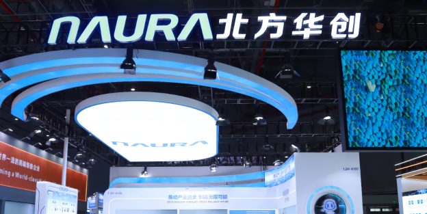
The event features China’s leading domestic chip equipment makers. As a major A-share player, Naura unveiled several new products. As noted by STAR Market Daily, its 12-inch NMC612H inductively coupled plasma (ICP) etching system delivers aspect ratios of several hundred to one for small-feature etching with angstrom-level uniformity, reinforcing its position in high-end ICP tools and supporting more advanced nodes.
The report also highlights that Naura’s 12-inch Qomola HPD30 hybrid bonding system places the company among the first in China to complete customer-side process verification for die-to-wafer (D2W) hybrid bonding, marking its entry into 3D integration hybrid bonding equipment.
AMEC also unveiled four new tools, expanding its capabilities in etching, thin-film deposition, and core intelligent components. Notably, as STAR Market Daily indicates, the launch of Primo Angnova™ provides a domestically controlled, advanced ICP etching solution for manufacturing logic chips at 5nm and below.
Meanwhile, ACM Research (Shanghai) introduced its ACM Planetary Family, a new product architecture comprising eight independent series named after the solar system’s eight planets, each corresponding to a core semiconductor process step. The company added that all newly showcased products have completed development and entered mass production, the report adds.
SiCarrier Shows Presence Through Subsidiaries
Still, SiCarrier, which made a strong debut at SEMICON 2025 with its lithography tool series named after well-known mountains, was unexpectedly absent this year, with subsidiaries Long Sight and Qiyunfang attending instead. As STAR Market Daily highlights, Qiyunfang has developed two electronic engineering EDA tools with fully proprietary intellectual property. Its solutions have served more than 20,000 engineers, with enterprise testing showing they can shorten time-to-market by 40%.
In one of the most closely watched segments, lithography equipment, STAR Market Daily notes that CFMEE showcased maskless direct-write solutions spanning panel-level to wafer-level applications. Its WLP series enables direct exposure without photomasks and supports wafer-level packaging, offering solutions for advanced packaging processes such as CoWoS- and SoW-like technologies.
Beyond China’s domestic players, global equipment makers are also showcasing new products at the event. According to The Asia Business Daily, Hanmi Semiconductor unveiled its “2.5D TC Bonder” for the first time at SEMICON China. As the report notes, the company plans to introduce its next-generation HBM production equipment, the “Wide TC Bonder,” in the second half of this year.
Read more
- [News] China Reportedly Ramps Up Chip Tool Push, Sets 70% Target by 2027; SMEE, NAURA at Forefront
- [News] Three Chinese Chip Toolmakers Reportedly Enter Global Top 20 as Naura Rises to Fifth by Sales
(Photo credit: Naura)


