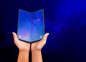
[News] China Advances TGV Glass Substrate Tech as BOE, ECHINT, and Peers Step Up
According to ijiwei, citing CNpowder, as chip packaging technology advances rapidly, glass substrate TGV (Through Glass Via) has emerged as a focal point of industry attention.
Glass substrates are gaining attention for their superior heat dissipation, conductivity, and flatness. As noted by Commercial Times, they reduce deformation risks compared with organic materials, making them essential for packaging large-die, high-power chips. The report further points out that in advanced applications such as server modules and silicon photonics, glass substrates are emerging as a strong alternative.
Chinese glass substrate TGV players such as 3D CHIPS, BOE, and Sky Semiconductor are actively developing related technologies and have already established multiple TGV packaging production lines. The following highlights some of the leading companies and their recent progress in this field.
3D CHIPS
3D CHIPS, a wholly owned subsidiary of Chengdu Micro-Technology, focuses on materials and integration technologies for 3D microsystems. As the report indicates, it was the first in the industry to propose TGV 3.0, achieving a breakthrough in sub-10-micron through-via and filling technology. In 2022, the company built a pilot line for TGV substrates and 3D integrated packaging.
BOE
Building on its expertise in display technology, BOE has developed semiconductor packaging solutions featuring TGV. The report notes that its new 8-inch pilot line is already in operation, with breakthroughs in areas such as high-density 3D interconnect and high aspect-ratio TGV. BOE has also introduced standard glass core substrates for AI chips, with mass production planned after 2026.
Sky Semiconductor
Sky Semiconductor focuses on advanced packaging and system integration. In TGV, its wafer-level packaging shipments have reportedly surpassed 20,000 units. As the report notes, the company achieved a breakthrough in 4-micron via diameter technology and, in 2024, mastered 2.5D high-density glass interposer technology. Its products now support large-chip packaging for AI, CPU, and GPU applications.
Guangdong Fozhixin Microelectronics
Guangdong Fozhixin Microelectronics specializes in panel-level fan-out packaging and glass substrate processing. In TGV, its minimum via diameter reaches 1 micron with an aspect ratio up to 150:1. The company has also built China’s first mass-production line for large panel-level fan-out packaging with independent intellectual property rights. Looking ahead, it plans to expand its glass-based chiplet solutions into broader application areas, the report notes.
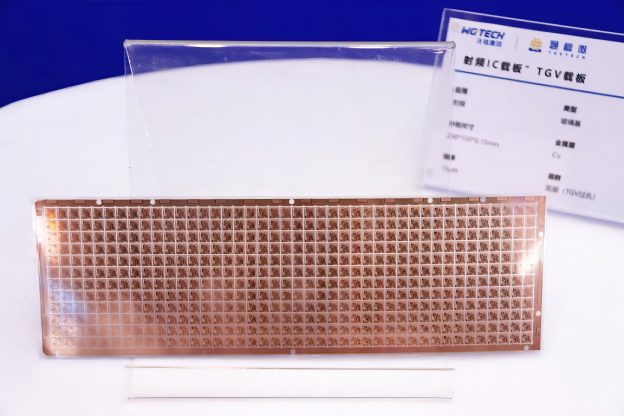
WG Tech
WG Tech’s operations span optoelectronic glass processing, backlight, and display modules, with glass-based advanced packaging substrates being one of its core businesses. Its wholly owned subsidiary, TGV TECH, is dedicated to the R&D and manufacturing of glass-based TGV multilayer precision circuit boards and related products.
Chengdu ECHINT
Chengdu ECHINT specializes in board-level advanced system-in-package (SiP) services, covering packaging design and chip packaging. In glass panel-level packaging, it was among the first in China to achieve mass production. As the report notes, in 2024 the company began volume production of its high-density FOMCM (Fan-Out Multi-Chip Module) platform, making it the only firm in China with this capability and marking a key advance in FOPLP (Fan-Out Panel-Level Packaging) packaging.
Read more
- [News] Tesla and Apple Reportedly Eye Glass Substrates, Lifting Prospects for Taiwanese Suppliers
- [News] Intel Reportedly Reaffirms Glass Substrate Roadmap, Pilot Line Rumored in 2025
(Photo credit: TGV TECH)
Please note that this article cites information from ijiwei, CNpowder, and Commercial Times.