[News] HBM Evolution Outpaces JEDEC Standards as Generation Cycles Reportedly Shrink to 2.5 Years
As the battle for next-gen HBM intensifies, memory giants are gearing up for a surge in demand from NVIDIA’s Rubin. According to ZDNet, NVIDIA plans to complete HBM4 final qualification tests in Q1 2026. However, EE Times notes that with the U.S. chipmaker racing ahead on GPU development, standards are struggling to keep pace, making customized HBM solutions essential to align with GPU and accelerator rollouts.
EE Times, citing Jin Yokoyama, senior director and memory product marketing manager at Advantest, highlights that unlike past memory transitions that took four to five years, HBM generations now evolve every two to two-and-a-half years.
The report, also citing Khurram Malik, Marvell’s senior director of product marketing, adds that the exponential growth of data due to robots, sensors, and other Internet of Things (IoT) edge devices has disrupted the traditional linear development of HBM, with HBM4E already coming to market within three years of the HBM3 specification being published by JEDEC.
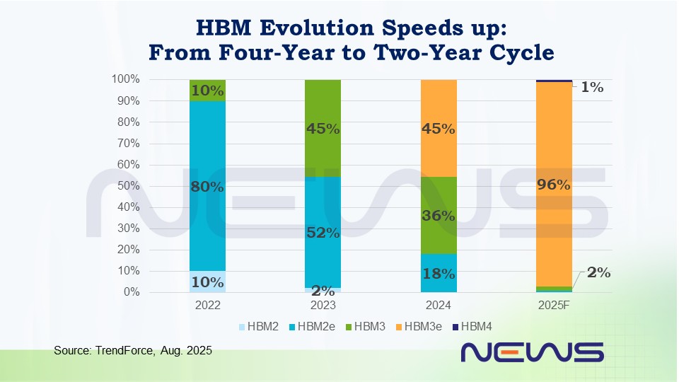
This scenario aligns with TrendForce’s projections, which show HBM3e’s share of total HBM output is expected to surge to 96% in 2025, up dramatically from 45% in 2024. Notably, the HBM3e output ratio was zero in 2023.
NVIDIA Pushes Faster HBM Iteration Amid GPU Ramp-Up
Therefore, as EE Times notes, traditionally governed by JEDEC standards, HBM is now seeing custom demands with HBM4, as SoC vendors and hyperscalers optimize features for AI ASICs and custom SoCs. More logic and controller functions are moving onto the HBM base die, produced at foundries like TSMC using 3nm and 5nm processes, the report suggests.
EE Times, citing Marvell, notes that NVIDIA, accelerating its GPU release cycle to once a year, plans to double memory bandwidth and capacity with each generation. With JEDEC standards lagging, the U.S. chip giant is therefore turning to custom HBM solutions.
In line with this trend, South Korean media outlet Hankyung reports that NVIDIA is working to reinforce its position in the HBM value chain by taking on the design of the HBM base die, starting in the second half of 2027.
Read more
- [News] Samsung Reportedly Passes NVIDIA HBM4 Sample Test, 30% HBM3E Discount to Challenge SK hynix
- [News] HBM Battle Heats Up: Micron Reportedly Hints 2026 Sell-Out, SK hynix Yet to Confirm
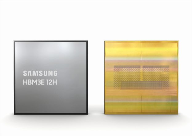
(Photo credit: Samsung)


