[News] Kioxia Begins BiCS 10 NAND Sampling, Reportedly Targets 2027 Mass Production at Kitakami Fab
Shortly after signaling summer sampling plans for its next-generation NAND, Kioxia on July 3 announced it has begun sample shipments of 1Tb (terabit) TLC (Triple-Level Cell) memory devices based on its 10th-generation BiCS FLASH 3D NAND technology. According to the company, the products will be manufactured at its Kitakami Plant Fab 2 in Iwate Prefecture, Japan.
According to Nikkei, Kioxia plans to begin BiCS 10 NAND mass production in 2027. Performance has been significantly upgraded, with data transfer speeds reaching 4.8 gigabits per second—about 30% faster than the previous generation. Memory density has increased by 60%, while read power efficiency has improved by roughly 30%, Nikkei reports.
Notably, The Japan Times reports that the new product, designed for solid-state drives (SSDs), is central to Kioxia’s strategy to capitalize on surging AI data center storage demand while reducing its reliance on smartphone-focused products, including those supplied to Apple.
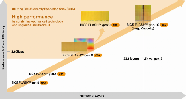
BiCS 10 Key Highlights: 332-Layer, CBA Technology
As reported by EE Times Japan, a key highlight of Kioxia’s 10th-generation BiCS FLASH is the strategic choice of a 332-layer architecture. Traditionally, the NAND industry has improved bit density and reduced costs by pushing toward higher layer counts, and competitors of Kioxia are also advancing development of products exceeding 400 layers, the report notes.
However, citing management, the report notes that excessive scaling of layer counts can create new challenges. According to Atsushi Inoue, General Manager of the Memory Business Division at Kioxia, at very high stack levels—such as above 400 layers—power consumption tends to increase as more memory layers are activated during read and write operations. In addition, further stacking may require thinner cell layers, which can reduce charge retention and raise concerns over long-term reliability.
Notably, Kioxia’s 332-layer NAND structure, according to EE Times Japan, can reduce cost per gigabyte by around 10% versus 400-plus-layer designs, while also delivering roughly 10% better power efficiency and about 35% higher memory cell reliability.
Another key feature of Kioxia 10th-generation BiCS FLASH is the continued use of CBA (CMOS directly Bonded to Array) technology, EE Times Japan suggests. Kioxia first introduced CBA in the 8th generation, which reportedly allowed the company to achieve interface speeds of 3.6Gb/s. According to Inoue, both the 9th and 10th generations now deliver 4.8Gb/s interface performance, extending Kioxia’s lead over rivals by roughly one year.
Rivals Speed up NAND Moves
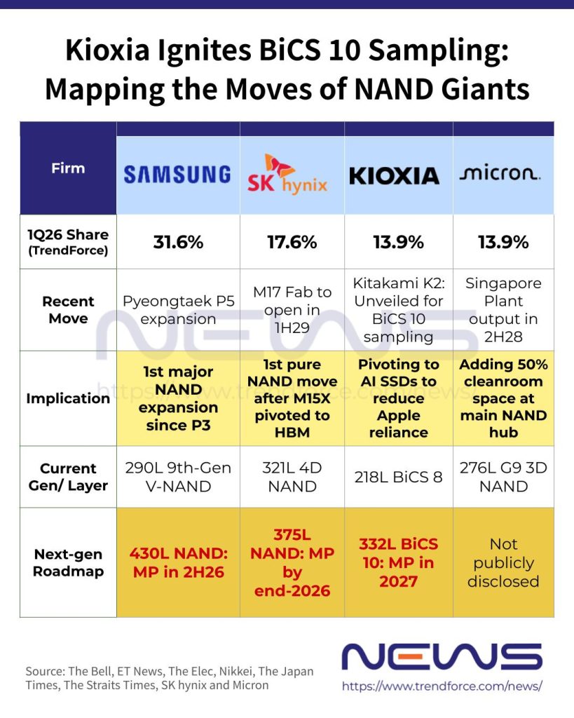
Notably, Kioxia’s progress comes as its South Korean rivals accelerate aggressive NAND capacity moves. On July 2, SK hynix announced plans to invest a total of 100 trillion won in Cheongju, with 80 trillion won allocated to its M17 NAND production facility, according to Chosun Biz.
CEO Kwak Noh-jung said NAND demand is rising rapidly while supply remains constrained, adding that Cheongju provides the fastest and most efficient base for SK hynix to build a new NAND fab, the report notes. According to SK hynix, construction of M17 is scheduled to begin next year, with operations targeted to commence in the first half of 2029.
Meanwhile, an April report from The Bell also suggested that Samsung plans to establish a new NAND production line at its Pyeongtaek Campus Plant 5 (P5), where the cleanroom is scheduled to be completed next year. If confirmed, this would mark the company’s first major NAND capacity expansion since P3, the report added.
Read more
- [News] Kioxia Adopts Cautious Capex Despite NAND Upcycle: Reportedly 10% Below FY23 Peak, Key Concerns in Focus
- [News] The Race to 400-Layer NAND: Roadmaps and Key Technologies Driving Samsung, SK hynix, and Kioxia
(Photo credit: Kioxia)