[News] LSTC’s Research Breakthrough Clarifies Sub-2nm Process Variations, Supporting Rapidus’s 1.4nm Ambitions
As Rapidus advances toward its roadmap of 2nm mass production in 2027 and 1.4nm in 2029, a new technology breakthrough could lend support to its ambitions. According to Hokkaido Shimbun, the Leading-edge Semiconductor Technology Center (LSTC), a consortium formed by national universities in Japan and other organizations, has established an analysis technology for next-generation semiconductors beyond the 2nm-class node.
LSTC notes that as line widths continue to shrink, traditional copper interconnects face mounting challenges, with rising electrical resistance leading to signal delay, higher power consumption, and increasingly severe heat dissipation issues. As a result, LSTC, in its press release on June 1, highlights that the project turns to ruthenium/air-gap (Ru/AG) interconnects, a leading candidate for sub-1nm logic nodes.
This initiative, carried out as an international collaborative research project among Yokohama National University (a quasi-member of LSTC), the University of Electro-Communications, and imec, clarifies how subtle manufacturing variations affect dielectric lifetime, while also establishing new design guidelines to improve reliability.
It is worth noting that LSTC shares a strategic alliance with Rapidus. According to Japan’s Ministry of Economy, Trade and Industry (METI), the country is executing a two-pronged national strategy to secure its next-generation semiconductor infrastructure beyond 2nm. This blueprint pairs LSTC as an open R&D hub for cutting-edge design, equipment, and materials, alongside Rapidus as the core manufacturing powerhouse.
Key Findings
According to LSTC, it has deep-dived into time-dependent dielectric breakdown (TDDB)—the phenomenon where insulating films degrade and fail over time. To test the waters, researchers deployed a dedicated structure packing ultra-fine 10nm ruthenium lines. By introducing air gaps with spacing from 10 to 14nm (hitting a tight 20–24nm metal pitch), they pushed the limits of reliability evaluation.
The results have reportedly confirmed that wider interconnect spacing leads to longer dielectric lifetime, which could be attributed to a reduction in the electric field between wires, which in turn lowers stress on the insulating film.
In addition, the study identifies clear within-chip variation: lifetime tends to be longer at the center of the wafer and shorter toward the edge, according to LSTC. This demonstrates that even nanoscale geometric variations introduced during fabrication can directly translate into differences in interconnect lifetime. As noted by LSTC, at a metal pitch of 22–24nm, such dimensional variations are the primary driver of lifetime variability.
According to LSTC, the findings quantitatively demonstrate that nanometer-scale structural variations during fabrication significantly influence the lifetime of ruthenium/air-gap interconnects. The study also establishes a first-of-its-kind framework for statistically predicting these effects, which enables reliability-aware design at and beyond the 2nm node, including sub-1nm technologies, where traditional evaluation methods are insufficient.
Read more
- [News] Rapidus Reportedly Taps Lam Research Panel-Level Packaging System for 600mm Square Glass Interposer Push
- [News] Rapidus Accelerates 1nm Push, Reportedly Targets Six-Month Gap with TSMC
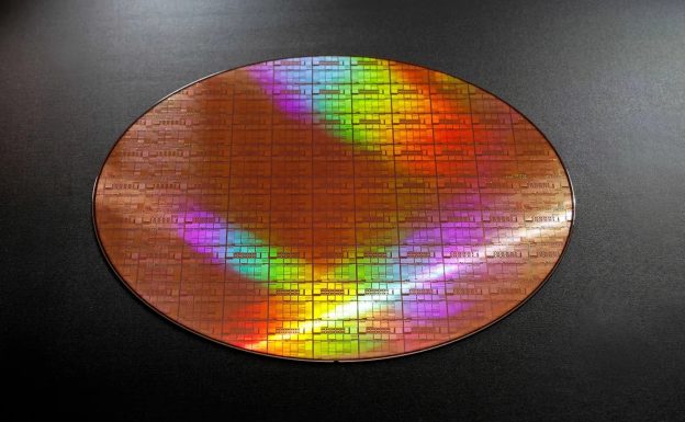
(Photo credit: Rapidus)


