


[News] Rapidus Reportedly Taps Lam Research Panel-Level Packaging System for 600mm Square Glass Interposer Push
As Lam Research announced the establishment of its Panel-Level Packaging Center of Excellence (CoE) in Salzburg, Austria, attention has turned to its customer and partner ecosystem.
According to EE Times Japan, Yasumitsu Orii, head of Rapidus’ engineering center, delivered a congratulatory video message at the event, noting that Rapidus is developing a 2.xD packaging technology that forms redistribution layers (RDL) on 600mm-square glass carriers, with Lam’s panel-level solutions—particularly its Kallisto electroplating system supporting 600mm panels—playing a key role.
As previously reported by Nikkei, Rapidus is not only targeting 2nm mass production in 2027 but is also advancing aggressively into advanced packaging. The company unveiled what it claims is the world’s first interposer prototype fabricated from a large-format glass substrate late last year, with mass production targeted for 2028, the report noted.
Orii’s latest remarks highlights Lam’s growing role in Rapidus’ advanced packaging efforts, as he described the two companies as trusted partners working closely to advance technology, EE Times Japan reports.
According to EE Times Japan, Lam Research already works with more than 50 customers and supports over five different panel sizes.
Lam Advances PLP from R&D to High-Volume Manufacturing
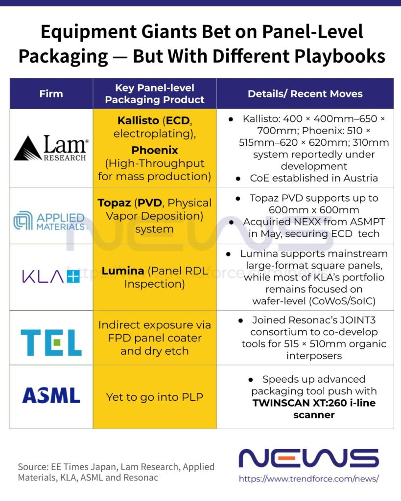
Notably, EE Times Japan reports that Lam showcased its Kallisto electroplating (ECD) system for panel-level packaging during a media tour of the new Salzburg facility. According to the company, Kallisto is tailored to address new challenges arising from large-panel formats, including warpage tolerance, co-planarity control, and process repeatability in high-volume manufacturing.
The system, as highlighted by the report, supports substrates ranging from 400mm × 400mm up to a maximum of 650mm × 700mm. It is also capable of enabling fine-line electroplating below 10μm for both single- and double-sided processing in organic and glass core technologies, the report adds.
While Kallisto reportedly targets R&D and low-volume production at around 30 panels per hour, Lam is already preparing for the next phase of panel-level packaging. According to EE Times Japan, its next-generation Phoenix platform is designed for high-volume manufacturing, quadrupling throughput to roughly 120 panels per hour. The system is said to be optimized for 510mm × 515mm panels and supports substrates up to 620mm × 620mm.
The move comes as the industry remains divided on panel formats. Reflecting this split, Lam is also developing a dedicated system for 310mm-square panels, with Corporate Vice President and Wet Equipment Technology Systems GM Aaron Fellis noting that both 310mm and 510mm formats are expected to coexist as mainstream standards for the foreseeable future, according to EE Times Japan.
Read more
- [News] Rapidus Reportedly Launches Back-End Prototype Line; Japan Adds ¥631.5B to Support 2nm Push
- [News] Rapidus Accelerates 1nm Push, Reportedly Targets Six-Month Gap with TSMC
(Photo credit: Lam Research)


